A method for peel off a perovskite oxide piezoelectric thin film on graphene by using a metal stress layer

A perovskite oxide and metal stress technology, which is applied in the manufacture of circuits, electrical components, semiconductors/solid-state devices, etc., can solve problems such as complex processes, impacts, and difficulty in satisfying thin films, and achieve the effect of smooth surfaces

Active Publication Date: 2019-01-08
XI AN JIAOTONG UNIV
View PDF8 Cites 4 Cited by
  • Summary
  • Abstract
  • Description
  • Claims
  • Application Information

AI Technical Summary

Problems solved by technology

At present, people's demand for the production of flexible electronic products is increasingly strong, but the current traditional thin film growth and processing methods are difficult to meet the needs of integrating materials on various flexible substrates.
In order to realize the integration of functional oxide films on flexible substrates, especially oxide piezoelectric films with a perovskite structure, some people directly grow films on flexible mica and other substrates, but this method will Limited to specific substrates such as mica, it is difficult to meet various practical needs; someone first grows a sacrificial layer that is easy to corrode on a hard substrate, and then grows a thin film layer that is expected to meet the functions of electronic devices on the sacrificial layer. The liquid corrodes the sacrificial layer so that the film floats on the corrosive liquid and is finally transferred to the flexible substrate. Although this method is not affected by the flexible substrate, the process is too complicated, and the corrosive liquid may have a certain impact on the film.

Method used


Image

  • A method for peel off a perovskite oxide piezoelectric thin film on graphene by using a metal stress layer
  • A method for peel off a perovskite oxide piezoelectric thin film on graphene by using a metal stress layer
  • A method for peel off a perovskite oxide piezoelectric thin film on graphene by using a metal stress layer

Examples


Embodiment 1

[0032] 1) Choose SiO interspersed with graphene 2 Barium titanate (BaTiO) grown on a Si substrate 3 , BTO) film;

[0033] 2) Load the sample and the Cr target into the magnetron sputtering film growth chamber;

[0034] 3) Evacuate the air pressure in the vacuum chamber to 5×10 -4 Below Pa, remove the pollutants adsorbed on the surface of the film;

[0035] 4) Pass high-purity argon gas into the vacuum chamber, and control the air pressure at 0.5Pa;

[0036] 5) Turn on the pulse power supply, control the power at 50W, grow for 5 minutes, increase the power to 150W, and grow for 2 hours;

[0037] 6) Turn off the pulse power supply, inject air into the cavity, and take out the sample;

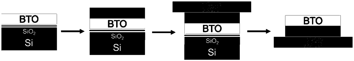
[0038] 7) Adhesive tape is attached to the surface of the sample obtained in step 6), and the tape is torn off the substrate to realize the peeling off of the film.

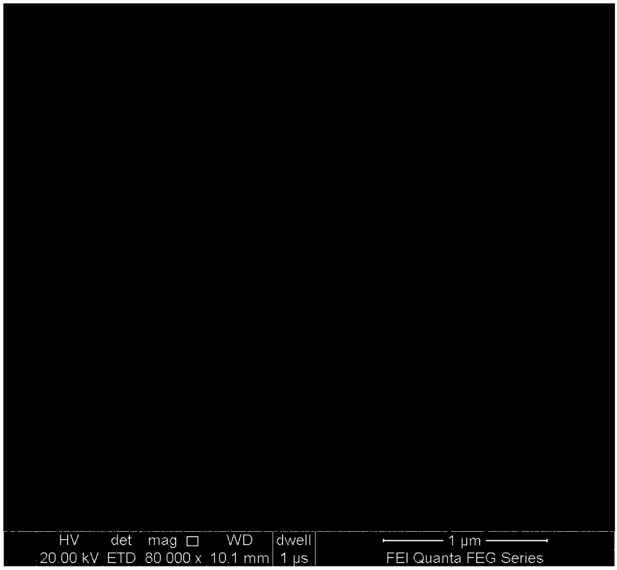
[0039] Such as figure 1 , the stripping process is shown below. Such as figure 2 , the peeled film is observed by SEM, an...

Embodiment 2

[0041] 1) Choose SiO interspersed with graphene 2 Barium titanate (BaTiO) grown on a Si substrate 3 , BTO) film;

[0042] 2) Load the sample and the Cr target into the magnetron sputtering film growth chamber;

[0043] 3) Evacuate the air pressure in the vacuum chamber to 5×10 -4 Below Pa, remove the pollutants adsorbed on the surface of the film;

[0044] 4) Introduce high-purity argon gas into the vacuum chamber, and control the air pressure at 0.3Pa;

[0045] 5) Turn on the pulse power supply, control the power at 40W, grow for 5 minutes, increase the power to 150W, and grow for 2 hours;

[0046] 6) Turn off the pulse power supply, inject air into the cavity, and take out the sample;

[0047] 7) Adhesive tape is attached to the surface of the sample obtained in step 6), and the tape is torn off the substrate to realize the peeling off of the film.

Embodiment 3

[0049] 1) Choose SiO interspersed with graphene 2 Barium titanate (BaTiO) grown on a Si substrate 3 , BTO) film;

[0050] 2) Load the sample and the Cr target into the magnetron sputtering film growth chamber;

[0051] 3) Evacuate the air pressure in the vacuum chamber to 5×10 -4 Below Pa, remove the pollutants adsorbed on the surface of the film;

[0052] 4) Pass high-purity argon gas into the vacuum chamber, and control the air pressure at 1.0Pa;

[0053] 5) Turn on the pulse power supply, control the power at 100W, grow for 10 minutes, increase the power to 200W, and grow for 2 hours;

[0054] 6) Turn off the pulse power supply, inject air into the cavity, and take out the sample;

[0055] 7) Adhesive tape is attached to the surface of the sample obtained in step 6), and the tape is torn off the substrate to realize the peeling off of the film.


PUM

PropertyMeasurementUnit
thicknessaaaaaaaaaa

Abstract

The invention discloses a method for stripping perovskite oxide piezoelectric thin film on graphene by using metal stress layer, comprising the following steps: 1) selecting perovskite oxide piezoelectric thin film grown on the graphene layer; 2) selecting metal Cr as that material of the metal stress layer; 3) in that growth proces of the Cr metal stress layer, the argon gas pressure is control to be 0.3 to 1.0 Pa; The Cr metal stress layer was grown at low power of 40-100W for 5 - 10min, and then grown at high power of 150W-200W for 2h. 4) the Cr stress layer / film / graphene / adhesive tape on the substrate obtained in the step 3), and tearing the adhesive tape off the substrate to realize the peeling off of the piezoelectric film. In order to simply prepare the perovskite oxide piezoelectric thin film with high quality on any flexible substrate, the invention realizes the peeling off of the perovskite oxide piezoelectric thin film and further completes the transfer of the thin film by utilizing the weak Van der Waals force and the metal stress layer formed by contacting the graphene with the three-dimensional material.

Description

technical field [0001] The invention relates to a method for peeling off a perovskite oxide piezoelectric thin film grown on graphene by using a metal stress layer. Background technique [0002] Thin film growth technology is the cornerstone of modern electronic products. The miniaturization of electronic products and the realization of functional diversification are inseparable from the development of thin film technology. At present, people's demand for the production of flexible electronic products is increasingly strong, but the current traditional thin film growth and processing methods are difficult to meet the integration of materials on various flexible substrates. In order to realize the integration of functional oxide films on flexible substrates, especially oxide piezoelectric films with a perovskite structure, some people directly grow films on flexible mica and other substrates, but this method will Limited to specific substrates such as mica, it is difficult t...

Claims


Application Information

Patent Timeline
Patent Type & Authority Applications(China)
IPC IPC(8): H01L21/033
CPCH01L21/0331
Inventor 牛刚代立言任巍赵金燕赵慧丰刘逸为刘学森王伟超武和平王延昆
Owner XI AN JIAOTONG UNIV
Why Eureka
Try Eureka