ESD protection circuit

An ESD protection and circuit technology, applied in the direction of emergency protection circuit devices, circuits, circuit devices, etc., can solve the problems of grid negative voltage test incompatibility, difficult reliability ESD tolerance, large conduction current, etc.

Active Publication Date: 2019-01-11
HUAWEI TECH CO LTD
View PDF5 Cites 16 Cited by
  • Summary
  • Abstract
  • Description
  • Claims
  • Application Information

AI Technical Summary

Problems solved by technology

[0005] However, since the above-mentioned ESD circuit conducts a large current when the gate and source of the P-type GAN enhanced power device 30 have a reverse voltage bias,

Method used


Image

  • ESD protection circuit
  • ESD protection circuit
  • ESD protection circuit

Examples


Embodiment Construction

[0028] In order to enable those skilled in the art to better understand the technical solutions in the embodiments of the present application, the technical solutions in the embodiments of the present application will be further described in detail below in conjunction with the accompanying drawings.

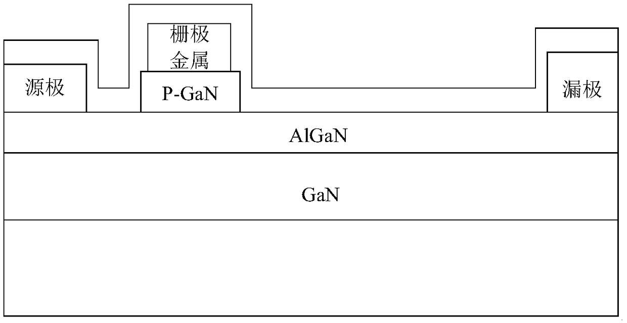
[0029] When negative ESD occurs on the gate of the P-type GaN enhanced power device, the ESD protection circuit in the traditional technology causes a large negative current in the gate of the P-type GaN enhanced power device. Negative leakage flooded. Therefore, when the traditional ESD protection circuit is adopted, the product reliability of the P-type GaN enhanced power device cannot be guaranteed. However, if the ESD protection circuit is not used, the pass rate of the P-type GaN enhanced power device will be lost to a certain extent. For this application, a new ESD protection circuit is proposed. It should be pointed out that unless otherwise specified, the enhancement-mo...


PUM


Abstract

An embodiment of the present application discloses an ESD protection circuit, comprising a negative ESD protection module and a positive ESD protection module, wherein the negative ESD protection module comprises a first resistor, a charging capacitor, a first field effect transistor and a second field effect transistor, and the positive ESD protection module comprises a fourth field effect transistor. When a negative ESD event occurs, the gate of P-type GAN enhanced power supply will have a large transient voltage relative to the source, so that a displacement current from the source to the gate of the P-type GAN enhanced power supply is generated on the recharge capacitor, as that first field effect transistor is tur on, the first field effect transistor and the second field effect transistor form a path, thereby releasing negative ESD energy from the grid relative to the source. At that same time, when a negative steady-state voltage is apply to the gate electrode with respect to the source electrode, the first field effect transistor is in an off state, so that the negative voltage test at the steady-state state can be compatible.

Description

technical field [0001] The present application relates to the field of semiconductor technology, in particular to an ESD protection circuit. Background technique [0002] Wide bandgap semiconductor power devices are power devices based on third-generation semiconductor materials, mainly including diamond power devices, silicon carbide SiC power devices, gallium nitride GaN power devices, etc. Among them, GaN power devices are widely used in the industry due to their advantages such as high breakdown electric field, high electron saturation velocity and high electron mobility in heterostructures. The current mainstream lateral GaN power device is based on the AlGaN / GaN heterojunction structure, through the introduction of a special gate structure to deplete the two-dimensional electron gas below the channel to achieve an enhanced (that is, normally-off device, defined as the threshold Voltage Vth>0) work has been applied to the power converter and its related driving circ...

Claims


Application Information

Patent Timeline
IPC IPC(8): H02H9/04
CPCH02H9/046H01L27/0248H01L27/0266
Inventor 蒋其梦李玉山王汉星
Owner HUAWEI TECH CO LTD
Why Eureka
Try Eureka