A flip-chip LED chip and a manufacturing method thereof

A LED chip and flip-chip technology, applied in the direction of electrical components, circuits, semiconductor devices, etc., can solve the problems of inability to effectively protect the chip process layer, metal thimble damage, etc., and achieve the effect of avoiding damage and good ductility

Active Publication Date: 2019-01-15
HC SEMITEK CORP
View PDF3 Cites 9 Cited by
  • Summary
  • Abstract
  • Description
  • Claims
  • Application Information

AI Technical Summary

Problems solved by technology

[0006] The embodiment of the present invention provides a flip-chip LED chip and its manufacturing method, which can sol

Method used


Image

  • A flip-chip LED chip and a manufacturing method thereof
  • A flip-chip LED chip and a manufacturing method thereof
  • A flip-chip LED chip and a manufacturing method thereof

Examples


Example Embodiment

[0050] In order to make the objectives, technical solutions, and advantages of the present invention clearer, the embodiments of the present invention will be described in further detail below in conjunction with the accompanying drawings.
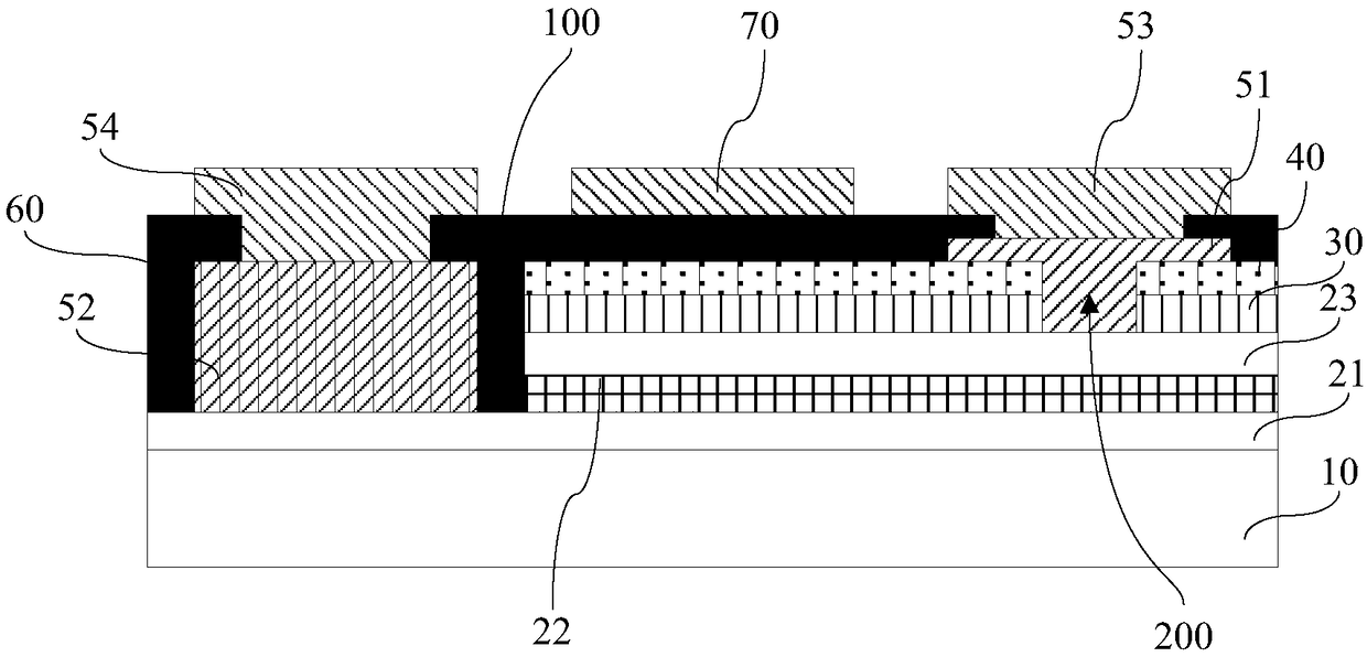
[0051] The embodiment of the present invention provides a flip-chip LED chip, figure 1 This is a schematic structural diagram of a flip-chip LED chip provided by an embodiment of the present invention, see figure 1 The flip-chip LED chip includes a substrate 10, an N-type semiconductor layer 21, an active layer 22, a P-type semiconductor layer 23, a transparent conductive film 30, a reflective layer 40, a P-type electrode 51, an N-type electrode 52, and a passivation layer. 60. P-type pad 53, N-type pad 54, and anti-thimble layer 70. The N-type semiconductor layer 21, the active layer 22 and the P-type semiconductor layer 23 are sequentially laminated on the substrate 10, and the P-type semiconductor layer 23 is provided with a groove 100 exte...


PUM

PropertyMeasurementUnit
Thicknessaaaaaaaaaa
Thicknessaaaaaaaaaa

Abstract

The invention discloses a flip-chip LED chip and a manufacturing method thereof, belonging to the field of semiconductor technology. The flip-chip LED chip comprises a substrate, an N-type semiconductor layer, an active layer, a P-type semiconductor layer, a transparent conductive film, a reflective layer, a P-type electrode, an N-type electrode, a passivation layer, a P-type pad, an N-type pad and an anti-pin layer; The P-type pad is arranged on the passivation layer around the P-type electrode and the region where the P-type electrode is located, and the N-type pad is arranged on the passivation layer around the N-type electrode and the region where the N-type electrode is located. The anti-thimble layer is arranged on the passivation layer between the P-type pad and the N-type pad; Theanti-thimble layer is formed of a metal material, and the anti-thimble layer is spaced between the P-type pad and the N-type pad. As that metal material is adopt to form the anti-thimble layer, the metal material has good ductility, the anti-thimble lay can effectively release the acting force of the metal thimble, the chip process layer is for with good protection, and the metal thimble can effectively prevent the chip process layer from being damaged by the metal thimble.

Description

technical field [0001] The invention relates to the technical field of semiconductors, in particular to a flip-chip LED chip and a manufacturing method thereof. Background technique [0002] Light Emitting Diode (English: Light Emitting Diode, referred to as: LED) is a semiconductor diode that can convert electrical energy into light energy. As a new type of light-emitting device, LED technology has developed rapidly, has a wide range of application fields, has strong industrial driving force, and has great energy-saving potential. It meets the requirements of low-carbon and ecological economy and the development trend of contemporary emerging industries. Compared with traditional electric lighting methods, LED lighting has the advantages of energy saving, environmental protection, longevity and high efficiency, and is recognized by various countries as the most promising high-efficiency lighting industry. [0003] The chip is the core component of the LED, which is divided...

Claims


Application Information

Patent Timeline
IPC IPC(8): H01L33/00H01L33/48H01L33/60H01L33/62
CPCH01L33/0091H01L33/48H01L33/60H01L33/62
Inventor 张威王江波
Owner HC SEMITEK CORP
Why Eureka
Try Eureka