A wideband low profile microstrip antenna

A microstrip antenna and low profile technology, applied in the field of wireless communication systems and broadband low profile microstrip antennas, can solve problems such as narrow bandwidth and limitations, and achieve the effects of widening bandwidth, reducing quality factor, and improving overall performance

Active Publication Date: 2019-01-15
XIDIAN UNIV
View PDF4 Cites 9 Cited by
  • Summary
  • Abstract
  • Description
  • Claims
  • Application Information

AI Technical Summary

Problems solved by technology

The antenna has a working bandwidth of 10% and a profile height of 3.124mm, which is 0.1λ ε (λ ε is the dielectric wavelength

Method used


Image

  • A wideband low profile microstrip antenna
  • A wideband low profile microstrip antenna
  • A wideband low profile microstrip antenna

Examples


Embodiment 1

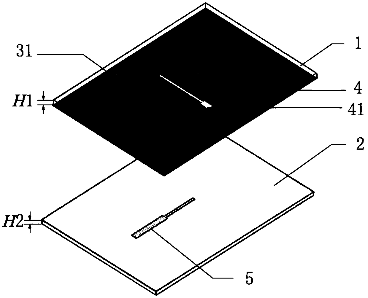
[0025] refer to figure 1 , a broadband low-profile microstrip antenna, including a first dielectric substrate 1 and a second dielectric substrate 2 stacked up and down, the thickness of the first dielectric substrate 1 is H1=0.508mm, and the dielectric constant ε 1 =3.48, the thickness H2 of the second dielectric substrate 2=0.254mm, the dielectric constant ε 2 =3.48; the upper surface of the first dielectric substrate 1 is printed with a radiation unit 3, and its structure is as follows figure 2 As shown, a metal floor 4 is printed on the lower surface, and a first rectangular slit 41 is etched on the metal floor 4, and its structure is as follows image 3 As shown; the lower surface of the second dielectric substrate 2 is printed with a microstrip feeder 5, and its structure is as follows Figure 4 Shown; the profile height of the antenna is 0.762mm.

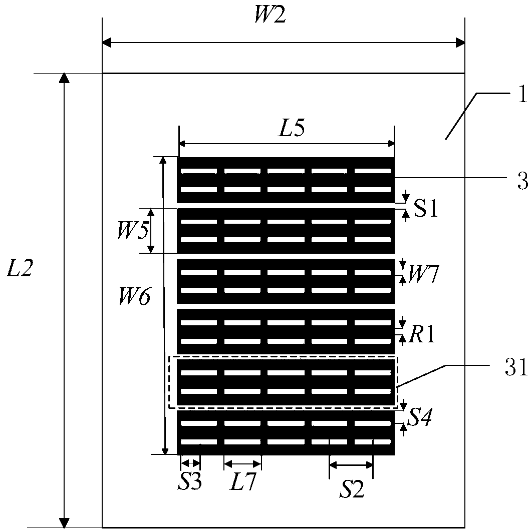
[0026] refer to figure 2 , the plate surface shape of the first dielectric substrate 1 is rectangular, its wide side d...

Embodiment 2

[0033] This embodiment has the same structure as Embodiment 1, only some parameters have been adjusted;

[0034] The number of rectangular patches 31 is N=3, the distance between adjacent rectangular patches 31 is S1=0.1mm, and the number of second rectangular slits in each row is M=3;

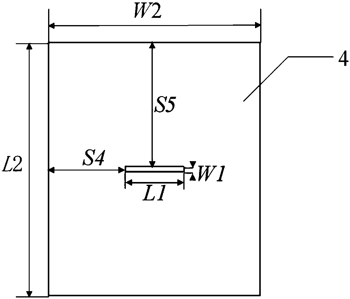
[0035] The wide side of the first rectangular slit 41 is W1=0.3mm, and the long side L1=4mm;

[0036] The wide side of the first dielectric substrate 1 is W2=17mm, the long side is L2=22mm, the thickness is H1=0.4mm, and the dielectric constant ε 1 =2, the thickness H2 of the second dielectric substrate 2=0.2mm, the dielectric constant ε 2 = 2;

[0037] The wide side of the first microstrip line 51 is W3=0.4mm, the long side L3=2.8mm, the wide side W4=0.16mm of the second microstrip line 52, and the long side L4=2.5mm.

Embodiment 3

[0039] This embodiment has the same structure as Embodiment 1, only some parameters have been adjusted;

[0040] The number of rectangular patches 31 is N=8, the distance between adjacent rectangular patches 31 is S1=0.3mm, and the number of second rectangular slits in each row is M=8;

[0041] The wide side of the first rectangular slit 41 is W1=0.6mm, and the long side L1=6mm;

[0042] The wide side of the first dielectric substrate 1 is W2=23mm, the long side is L2=26mm, the thickness is H1=0.6mm, and the dielectric constant ε 1 =6, the thickness H2 of the second dielectric substrate 2=0.3mm, the dielectric constant ε 2 = 6;

[0043] The wide side of the first microstrip line 51 is W3=0.6mm, the long side L3=3.5mm, the wide side W4=0.3mm of the second microstrip line 52, and the long side L4=3.2mm.

[0044] Below in conjunction with simulation experiment, technical effect of the present invention is described further:

[0045] 1. Simulation conditions and content:

[0...


PUM

PropertyMeasurementUnit
Thicknessaaaaaaaaaa
Thicknessaaaaaaaaaa
Thicknessaaaaaaaaaa

Abstract

A wideband low profile microstrip antenna aimed at ensuring low profile characteristics, widen the bandwidth of microstrip antenna, includes a first dielectric substrate and a second dielectric substrate stacked in a rectangular shape, a radiation unit is printed on the upper surface of the first dielectric substrate, the radiating element comprises N rectangular patches arranged in parallel, tworows of second rectangular slots parallel to the long sides of the rectangular patch are etched thereon, the number of each row of second rectangular slots is M, a metal floor is printed on the lowersurface of the first dielectric substrate, the metal floor is etched with the first rectangular slots, the rectangular patch is connected with the metal floor through M metallized vias, and a microstrip feed line is printed on the lower surface of the second dielectric substrate; The invention not only ensures the low profile characteristic of the microstrip antenna, but also widens the working bandwidth of the microstrip antenna, and can be used in a wireless communication system.

Description

technical field [0001] The invention belongs to the technical field of antennas, and relates to a wide-band low-profile microstrip antenna, which can be applied to wireless communication systems. Background technique [0002] With the development of wireless communication systems, people's requirements for antenna functions are increasing day by day. The microstrip antenna is an antenna formed by attaching a conductor sheet to a dielectric substrate with a conductor ground plate. It uses a microstrip line or a coaxial line to feed power, and excites a radio frequency electromagnetic field between the conductor patch and the ground plate, and passes through The gap between the perimeter of the patch and the ground plane radiates outward. Due to the advantages of small size, light weight, easy integration and low manufacturing cost, microstrip antennas are widely used in wireless communication systems and other fields. [0003] For traditional microstrip antennas, the lower ...

Claims


Application Information

Patent Timeline
IPC IPC(8): H01Q1/38H01Q1/48H01Q1/50H01Q9/04
CPCH01Q1/38H01Q1/48H01Q1/50H01Q9/045
Inventor 李龙易浩赵玉颖
Owner XIDIAN UNIV
Why Eureka
Try Eureka