

A preparation method and a product of a fatigue-resistant flexible electronic device
A flexible electronic device, fatigue resistance technology, applied in piezoelectric devices/electrostrictive devices, piezoelectric/electrostrictive/magnetostrictive devices, electrical components, etc., can solve waste, poor fatigue performance, and devices cannot Long-term use and other issues, to achieve the effect of easy operation, ultimate elongation and fatigue resistance, and reduce stress concentration
- Summary
- Abstract
- Description
- Claims
- Application Information
AI Technical Summary
Problems solved by technology
Method used
Image

Examples
preparation example Construction
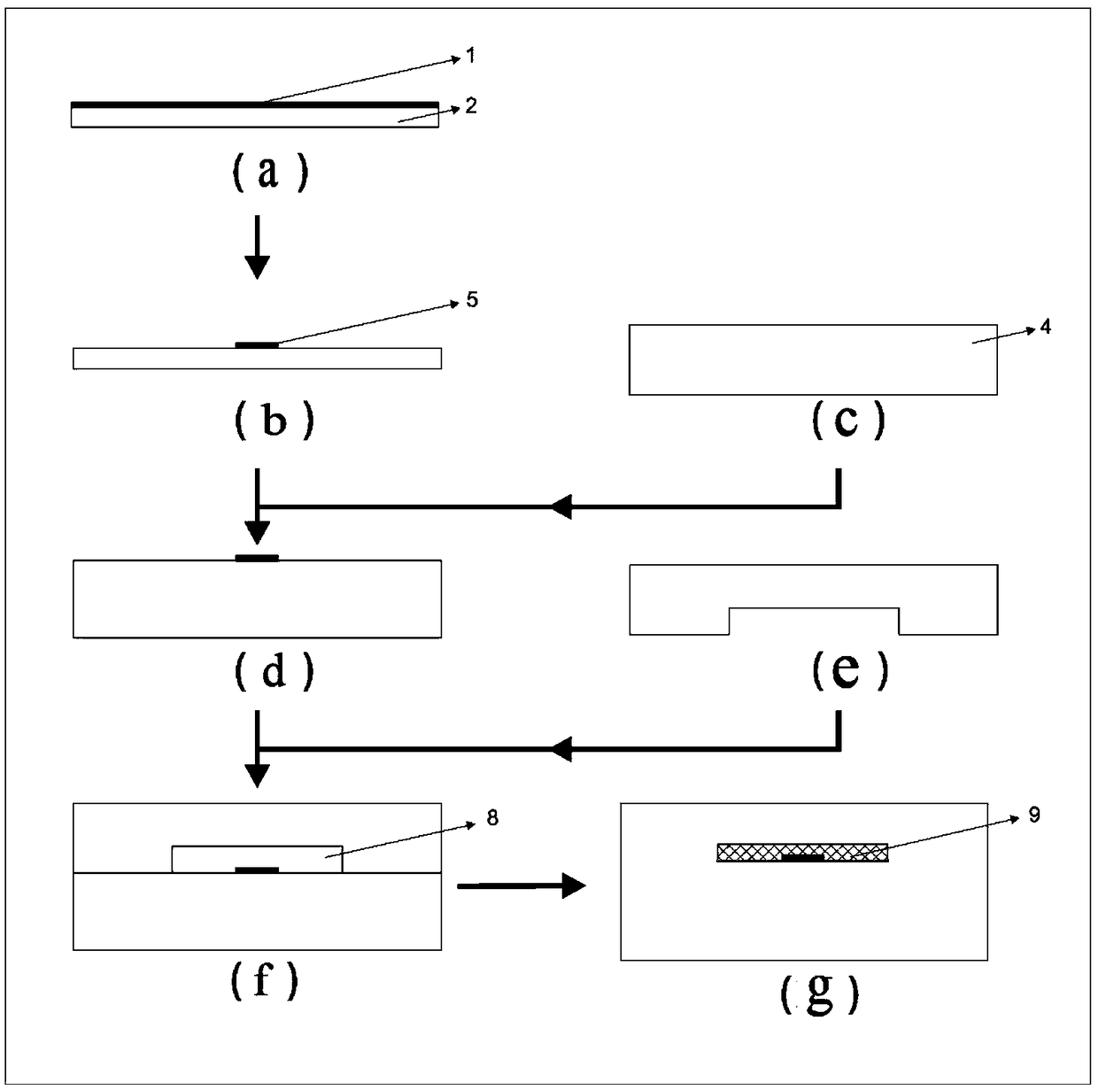
[0056] An embodiment of the present invention provides a method for preparing a fatigue-resistant flexible electronic device, which includes the following steps: including the following steps:
[0057] S1: Depict the shape and structure of the electrode material on the auxiliary substrate to obtain the electrode patterned thin film structure;
[0058] S2: constructing electrode material movable channels around the electrode patterned film structure by using a dissolution method or an etching method;
[0059] S3: Injecting a flexible material into the movable channel, and encapsulating the entrance and exit of the movable channel to obtain a fatigue-resistant flexible electronic device.
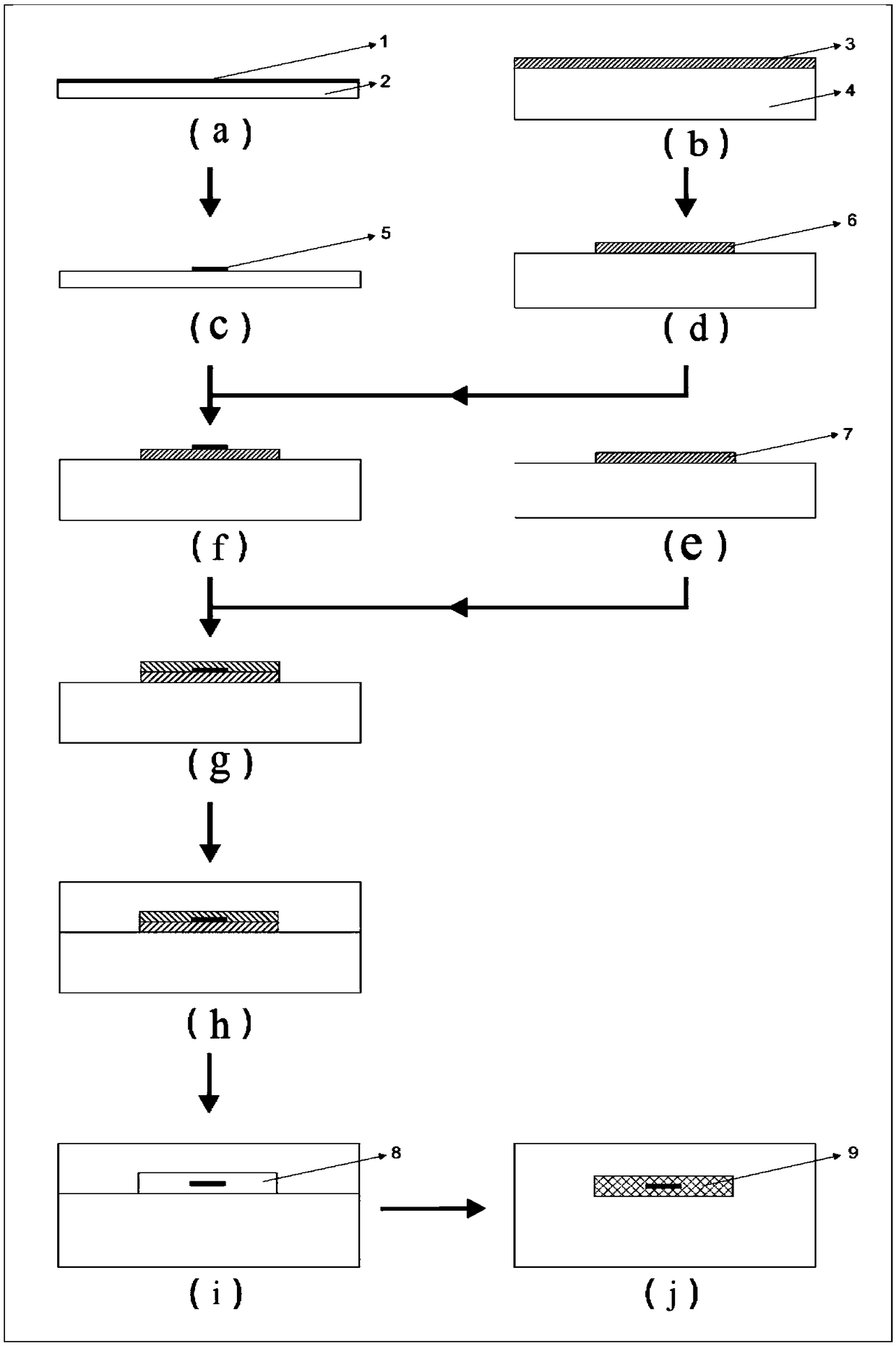
Embodiment 1
[0061] Such as figure 1 , such as 4 and Figure 5 As shown, the specific steps are as follows:
[0062] Adhere the electrode material on the heat-cured auxiliary substrate, adhere the organic soluble film on the heat-cured target substrate, and use laser, cutting, photolithography and other techniques to pattern the electrode material and organic soluble film The desired shape of the electrode and the shape of the organic soluble film are obtained, so as to obtain the auxiliary substrate of the electrode patterned film structure and the target substrate of the organic soluble film. Among them, metal electrodes are mostly designed in a serpentine shape, while polymer electrodes are mostly designed in a linear shape, and the shape of the organic soluble film matches the shape of the electrode patterned film structure.
[0063] The electrode patterned film structure placed on the auxiliary substrate is wetted and pressed against the organic soluble film target substrate, the el...
Embodiment 2
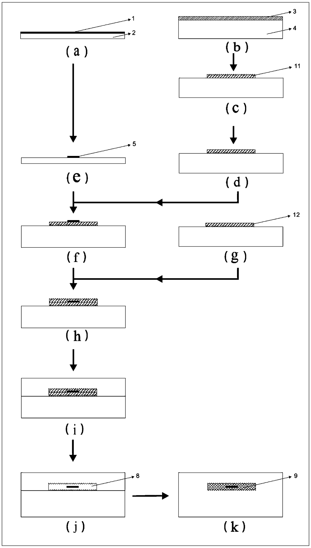
[0067] Such as figure 2 , such as 6 and Figure 7 As shown, the specific steps are as follows:
[0068] The electrode material 1 is adhered to the auxiliary substrate 2 by controlling the heating and curing time of the flexible polymer forming the auxiliary substrate 2 and the target substrate 4 so that it has a certain viscosity. The electrode material 1 is processed into a predetermined electrode patterned thin film structure by using methods such as laser, cutting or etching, such as Figure 6 As shown, the electrode patterned thin film structure auxiliary substrate was obtained.
[0069] Construction of a movable channel structure: With the help of transfer printing technology, the auxiliary substrate of the electrode patterned film structure is relatively pressed against the target substrate. Since the viscosity between the electrode patterned film structure 5 and the auxiliary substrate 2 is small, the electrode patterned film structure can be The structure 5 is tran...
PUM
| Property | Measurement | Unit |
|---|---|---|
| Thickness | aaaaa | aaaaa |
| Thickness | aaaaa | aaaaa |
| Thickness | aaaaa | aaaaa |
Abstract
Description
Claims
Application Information