The invention relates to a method for creating and querying a PCB component packaging library

A technology of device packaging and query methods, applied in network data query, instruments, file systems, etc., can solve problems such as poor reusability, difficulty in effective query, and difficulty in providing effective query results

Inactive Publication Date: 2019-01-18
UNIV OF ELECTRONICS SCI & TECH OF CHINA
View PDF7 Cites 19 Cited by
  • Summary
  • Abstract
  • Description
  • Claims
  • Application Information

AI Technical Summary

Problems solved by technology

[0004] However, the reusability of component packaging design at this stage is poor, and packaging engineers need to create it repeatedly every time. The main reasons are: first, the lack of effective management of packaging files, and

Method used


Image

  • The invention relates to a method for creating and querying a PCB component packaging library
  • The invention relates to a method for creating and querying a PCB component packaging library
  • The invention relates to a method for creating and querying a PCB component packaging library

Examples


Embodiment

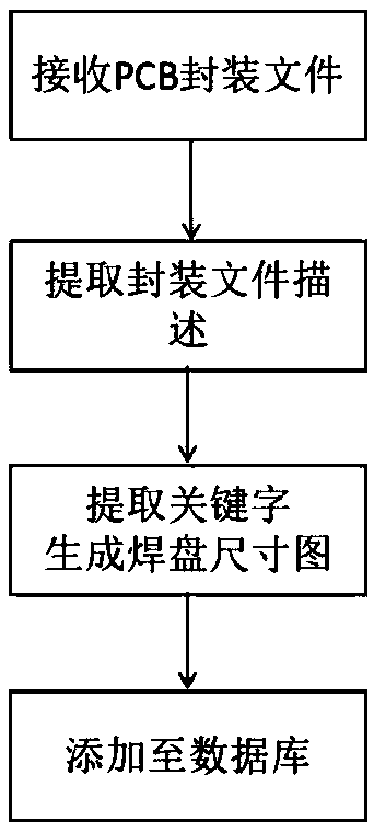
[0044] Figure 10 It is a flowchart of a method for creating and querying a PCB component packaging library in the present invention.

[0045] In this example, if Figure 10 As shown, a method for creating and querying a PCB component packaging library of the present invention comprises the following steps:

[0046] S1. Establish PCB component package description specification

[0047] A PCB component package contains information such as device shape, pad information, etc. Therefore, it is necessary to use a standardized package description specification for packaging. The PCB component package description specification adopts the following form: feature-characteristic value, graphic object-attribute name - attribute value - derived attribute - derived attribute value;

[0048] Example: Number: 1

[0049] Device Type:

[0050] Total number of PINs: xx;

[0051] Minimum PIN spacing: xx;

[0052] Assembly method: surface mount;

[0053] ...

[0054] Graphics object:

...

example

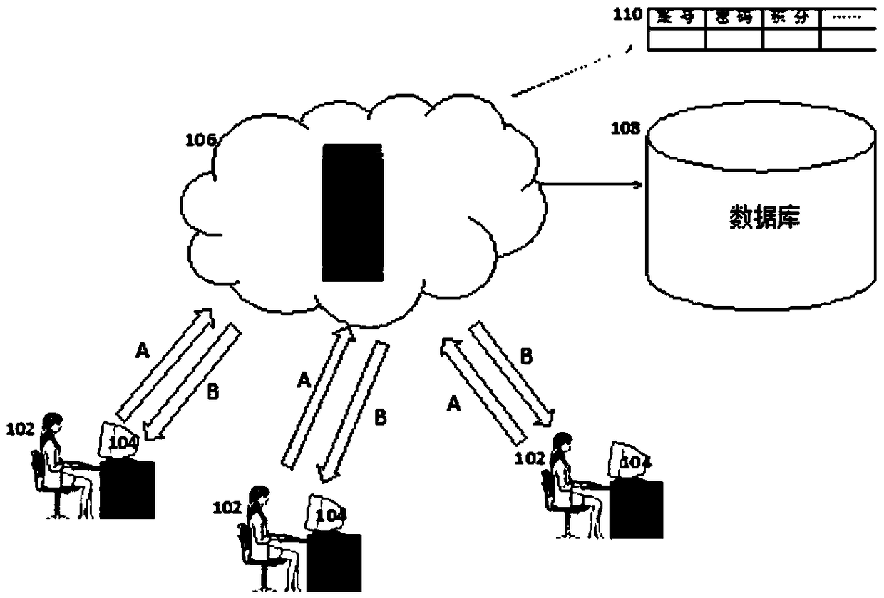
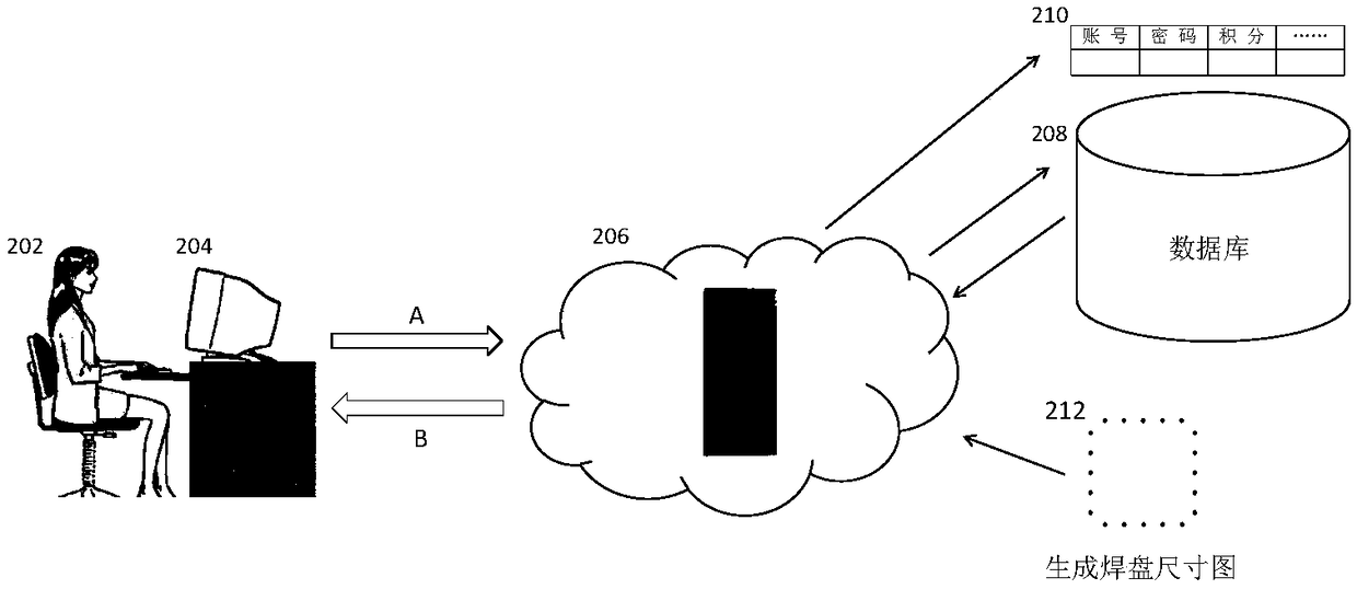
[0086] In this embodiment, the PCB device package library is created by crowdsourcing, and includes query text strings and systems and technologies that use various image understanding and graphic matching techniques to provide direct query and fuzzy query help for the device package library. In some examples, the user can automatically upload the package description file by installing the plug-in locally; or manually upload the EDA package library source file. When the server receives the source file of the EDA package library, the source file of the EDA package library will be automatically converted into a package description file. Extract from the package description file, including device model, mounting method, device shape, device shape length, width, PIN number, characteristic PIN spacing, pad coordinates, pad size, pad shape, pin position, and generate pad size Figure and package description file numbers, generate database records, add to SQL database. The conversion...


PUM


Abstract

The invention discloses a method for creating and querying a PCB component packaging library, which includes: generating a PCB component packaging description file through a defined device packaging description specification; Receiving a file stream at a server system, extracting an encapsulation description file, generating multi-dimensional retrieval keywords according to the encapsulation description file, and establishing a PCB component encapsulation library; receiving the query request and query condition by the server system, preferably directly querying by device model; then screeningand searching by using other keywords, and then extracting the first-order or high-order pad geometric features by combining digital image processing and graphics matching technology, and carrying out fuzzy query; Finally, generating EDA package library source files in the specified format from queried packaged description file, and providing the query results to the user.

Description

technical field [0001] The invention belongs to the technical field of electronic design automation, and more specifically relates to a method for creating and querying a package library of PCB components. Background technique [0002] The electronic circuit design process is very complex, mainly including system specification, architecture design, function and logic design, circuit design, physical design, physical verification, manufacturing, packaging and testing. Before carrying out operations such as chip planning, layout, and wiring in physical design, it is necessary to complete the packaging library design of components, that is, to construct the footprint of electronic components, including pins, dimensions, etc., for circuit board design. [0003] Packaging technology directly affects the performance of the device itself and the design and manufacture of PCB (printed circuit board), so it is very important. There are many kinds of electronic components, including ...

Claims


Application Information

Patent Timeline
IPC IPC(8): G06F16/18G06F16/953G06F16/13G06F16/14G06F17/50
CPCG06F30/39
Inventor 郑亚莉潘力立
Owner UNIV OF ELECTRONICS SCI & TECH OF CHINA
Why Eureka
Try Eureka