Array substrate, making method thereof and display panel

The technology of an array substrate and a manufacturing method is applied in the field of an array substrate, a manufacturing method thereof and a display panel, which can solve the problems of increased production cost and increased manufacturing process, and achieve the effects of reducing the production cost, reducing the process and saving the production cycle.

Inactive Publication Date: 2019-01-25
CHENGDU ZHONGDIAN PANDA DISPLAY TECH CO LTD
View PDF4 Cites 0 Cited by
  • Summary
  • Abstract
  • Description
  • Claims
  • Application Information

AI Technical Summary

Problems solved by technology

[0005] In view of the above-mentioned defects in the prior art, the present invention provides an array substrate and its manufacturing method and a display panel, so as to solve the technical problems of increasing the manufacturing process of the array substrate or the color filter substrate and increasing the production cost of the existing PS preparation

Method used


Image

  • Array substrate, making method thereof and display panel
  • Array substrate, making method thereof and display panel
  • Array substrate, making method thereof and display panel

Examples


Embodiment 1

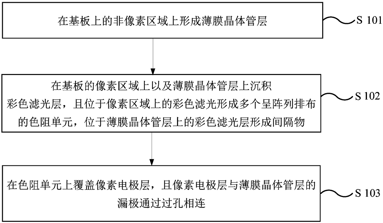
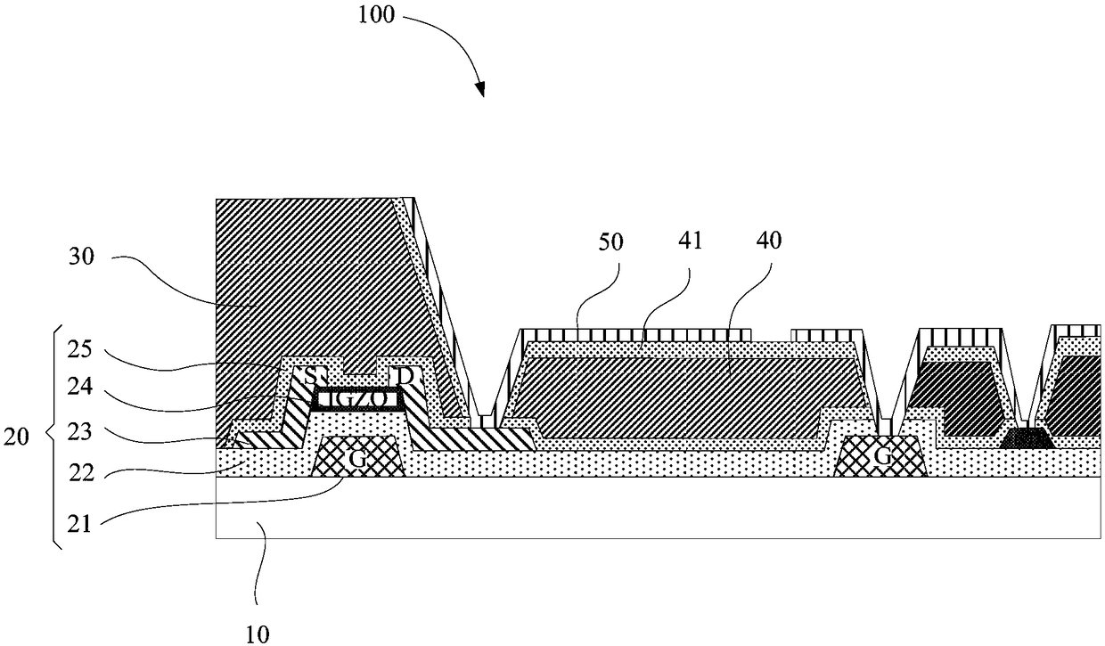
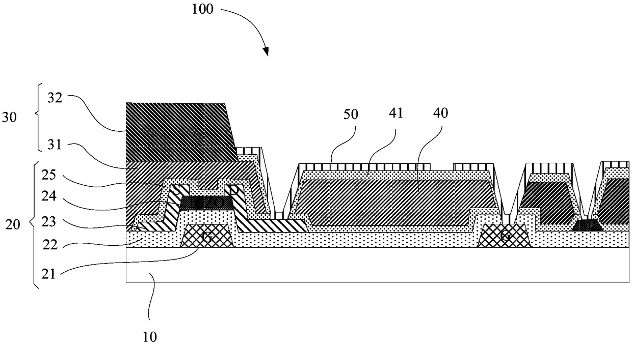
[0070] figure 1 It is a schematic flowchart of the manufacturing method of the array substrate provided by Embodiment 1 of the present invention, figure 2 A schematic structural view of the array substrate provided by the present invention, image 3 Another structural schematic diagram of the array substrate provided by the present invention, Figure 4 Another structural schematic diagram of the array substrate provided by the present invention;

[0071] This embodiment provides a method for manufacturing an array substrate, specifically an array substrate (color filter on array, COA for short) provided with a color filter, that is, a COA array substrate. In this embodiment, the array substrate used The spacer (PS) is formed simultaneously in the process of forming the color filter on the color filter, thereby avoiding setting up the PS process independently to form the PS. The number of steps in the process is reduced, thereby reducing production costs.

[0072] Wherein,...

Embodiment 2

[0117] This embodiment provides an array substrate 100, the array substrate 100 is manufactured by using the preparation method of any one of the above embodiments, see Figure 2-4 As shown, the array substrate 100 includes: a thin film transistor layer 20 disposed on the substrate 10, a plurality of color resistance units 40 arranged in an array, and a drain covering the color resistance units 40 and connected to the drain of the thin film transistor layer 20. The pixel electrode layer 50, and the spacer 30 is arranged on the thin film transistor layer 20, wherein, in this embodiment, since the PS is formed at the same time as the preparation of the color resistance unit 40, the manufacturing process of the array substrate 100 is reduced, and the Production cost, wherein, in this embodiment, since the color-resist unit 40 is located on the array substrate 100 , the array substrate 100 is specifically a COA array substrate 100 .

[0118] Wherein, in this embodiment, each color...

Embodiment 3

[0122] Figure 5 It is a schematic structural diagram of a display panel provided by Embodiment 3 of the present invention.

[0123] This embodiment provides a display panel 200, such as Figure 5 As shown, the display panel 200 includes the above-mentioned array substrate 100, the opposite substrate 60 arranged in a box with the array substrate 100, and the liquid crystal filled between the array substrate 100 and the opposite substrate 60, wherein the spacer on the array substrate 100 One end of 30 is abutted against the common electrode or black matrix on the opposite substrate 60. In the embodiment, since the color resist unit 40 is arranged on the array substrate 100, that is, the color filter layer is located on the array substrate 100, the color filter There is no need to arrange color filters on the substrate 10, so as Figure 4 As shown, the opposite substrate 60 opposite to the array substrate 100 includes a black matrix (Black Matrix, BM for short) 62 disposed on ...


PUM


Abstract

The invention discloses an array substrate, a making method thereof and a display panel. The method comprises the steps that a thin film transistor layer is formed on a non-pixel area on the substrate; color filter layers are formed on a pixel area of the substrate and the thin film transistor layer, the color filter layer located on the pixel area forms multiple color resistance units arranged inan array, and the color filter layer located on the thin film transistor layer forms a spacer; a pixel electrode layer covers the color resistance units, and drain electrodes of the pixel electrode layer and the thin film transistor layer are connected through via holes. According to the making method of the array substrate, the purpose of omitting the PS process is achieved, and the technical problems that by means of existing PS preparation, the making processes of the array substrate or a color film substrate are increased, and the production cost is increased are solved.

Description

technical field [0001] The present invention relates to the field of display technology, in particular to an array substrate, a manufacturing method thereof, and a display panel. Background technique [0002] Liquid crystal display (Liquid Crystal Display, LCD) is the most widely used display product on the market at present, and the liquid crystal display mainly includes a liquid crystal display panel and a backlight module. The liquid crystal between the (array) substrate and the color filter (color filter, CF for short) substrate, wherein, in order to maintain the distance between the two substrates, a spacer (photospacer, PS for short) is arranged between the CF substrate and the array substrate. [0003] At present, there are mainly two ways to arrange the spacer (PS): one is to form the PS on the side of the CF substrate facing the array substrate, specifically, to form the PS on the common electrode of the CF substrate; the other is to form the spacer on the array sub...

Claims


Application Information

Patent Timeline
Patent Type & Authority Applications(China)
IPC IPC(8): G02F1/1335G02F1/1362
CPCG02F1/133514G02F1/133512G02F1/136209G02F1/136227
Inventor 周天奇
Owner CHENGDU ZHONGDIAN PANDA DISPLAY TECH CO LTD
Why Eureka
Try Eureka