MOS type power device and preparation method thereof

A technology for power devices and well regions, which is used in semiconductor/solid-state device manufacturing, semiconductor devices, electrical components, etc. It can solve the problem of uneven channel current density, unoptimized channel length, well depth and channel The length cannot reach the optimal value at the same time, etc.

Pending Publication Date: 2019-01-25
BYD SEMICON CO LTD
View PDF8 Cites 2 Cited by
  • Summary
  • Abstract
  • Description
  • Claims
  • Application Information

AI Technical Summary

Problems solved by technology

[0009] However, the P-well region formed by the existing UMOS trench gate structure technology is a deep well planar junction. The characteristic of this well region is that the well depth and channel length cannot reach the optimal value at the same time.
In order to ensure sufficient withstand voltage of the device, the well depth should be at a minimum value, but the channel length cannot be optimized in this way.
And the deepe

Method used


Image

  • MOS type power device and preparation method thereof
  • MOS type power device and preparation method thereof
  • MOS type power device and preparation method thereof

Examples


Embodiment Construction

[0021] Embodiments of the present invention are described in detail below. The embodiments described below are exemplary only for explaining the present invention and should not be construed as limiting the present invention. If no specific technique or condition is indicated in the examples, it shall be carried out according to the technique or condition described in the literature in this field or according to the product specification. The reagents or instruments used were not indicated by the manufacturer, and they were all commercially available conventional products.

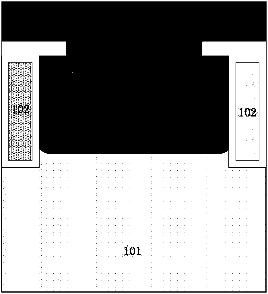
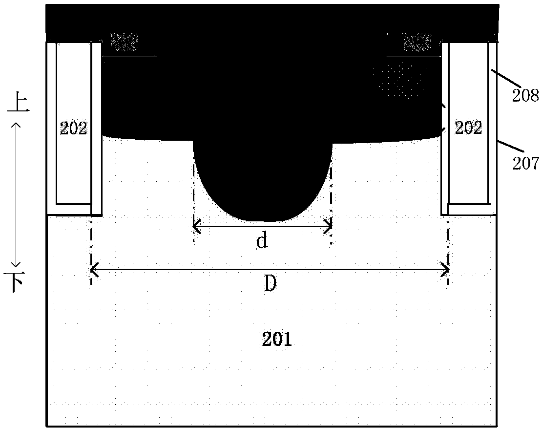
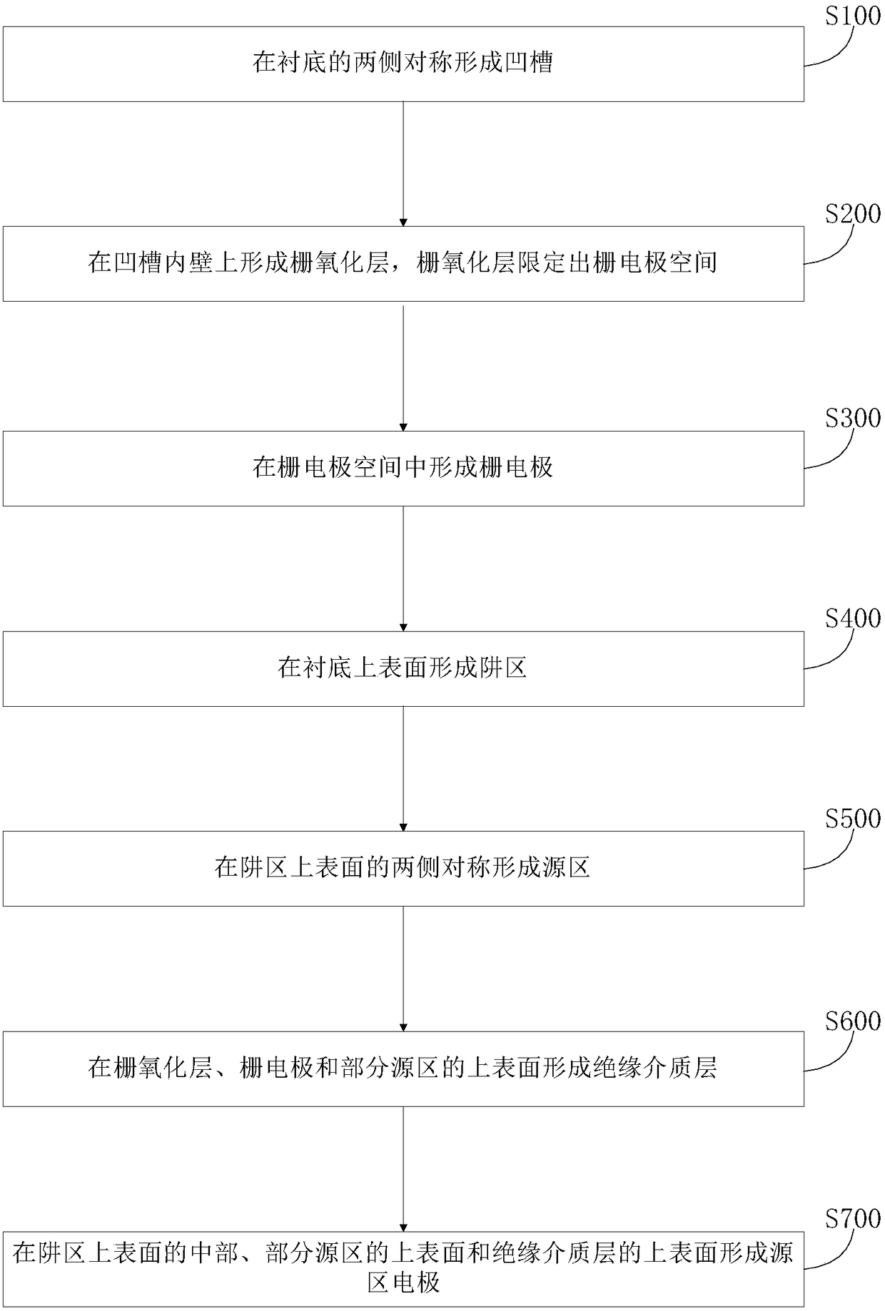
[0022] In one aspect of the invention, the invention provides a MOS type power device. According to an embodiment of the present invention, refer to figure 2 , the MOS type power device includes: a substrate 201; a well region 203, the well region 203 is arranged on the upper surface of the substrate 201, and the lower surface of the well region 203 is provided with a protrusion extending downward; a so...


PUM

PropertyMeasurementUnit
Channel lengthaaaaaaaaaa

Abstract

The invention provides a MOS type power device and a preparation method thereof. A MOS-type power device comprises a substrate; a Well region; a Source region; a Gate oxide layer; a Gate electrode; anInsulating dielectric layer; A source region electrode, wherein a lower surface of the well region is provided with a protrusion extending downward. Thus, the MOS type power device has a well depth deep enough, sufficient withstand voltage margin can be ensured, At the same time, it has enough short channel and lower saturation voltage drop to increase channel density and reduce channel short-circuit current, effectively reduce on-resistance and improve short-circuit safety ability, fully ensure the reliability of device application, and has quasi-channel current self-pinch-off function to enhance the high-voltage and large-current shutdown ability of the device.

Description

technical field [0001] The invention relates to the technical field of semiconductor devices, in particular to a MOS type power device and a preparation method thereof. Background technique [0002] Saturation voltage drop and turn-off energy together constitute the "overall figure of merit (FOM)" to measure the performance of MOS power devices. However, the saturation voltage drop is greatly affected by the channel condition. The voltage drop across the channel is inversely proportional to the channel width and directly proportional to the channel length, so to reduce on-state power dissipation, the channel length should be as short as possible. But on the other hand, the channel length must be able to ensure the breakdown voltage, which limits the minimum allowable value of channel length reduction. In addition, the channel length also has the effect of limiting the short-circuit current, so as to avoid the device from being burned out in the case of a short-circuit of th...

Claims


Application Information

Patent Timeline
IPC IPC(8): H01L29/78H01L29/06H01L29/10H01L29/423H01L21/336
CPCH01L29/0611H01L29/1033H01L29/4236H01L29/66666H01L29/7827
Inventor 秦博肖秀光吴海平
Owner BYD SEMICON CO LTD
Why Eureka
Try Eureka