On-chip micro electron source and manufacturing method thereof

An electron source and miniature technology, applied in the field of electronic science and technology, can solve the problem of small emission current and achieve the effect of improving heat dissipation

Pending Publication Date: 2019-01-29
PEKING UNIV
View PDF8 Cites 8 Cited by
  • Summary
  • Abstract
  • Description
  • Claims
  • Application Information

AI Technical Summary

Problems solved by technology

However, the overall emission current of the existing on-chip micro-electron sources is small, and it is difficult to meet more application requirements

Method used


Image

  • On-chip micro electron source and manufacturing method thereof
  • On-chip micro electron source and manufacturing method thereof
  • On-chip micro electron source and manufacturing method thereof

Examples


Embodiment 1

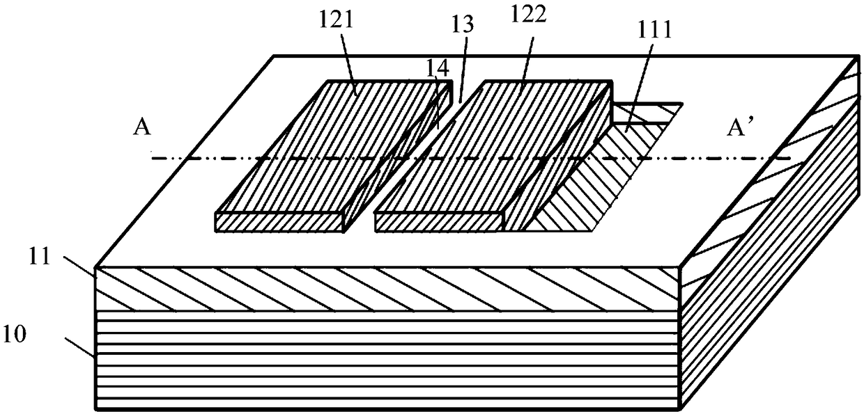
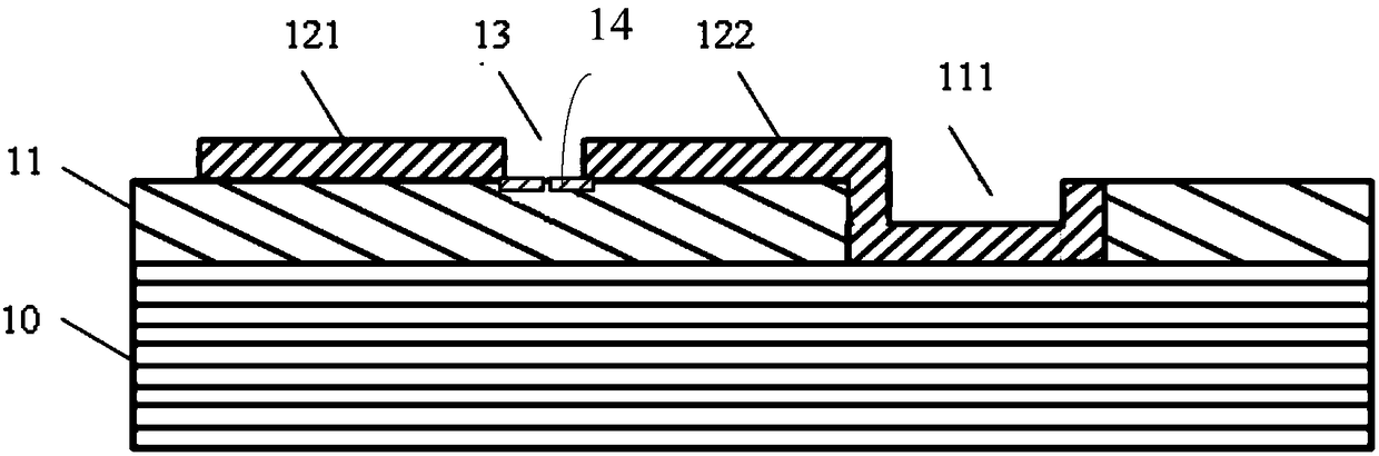
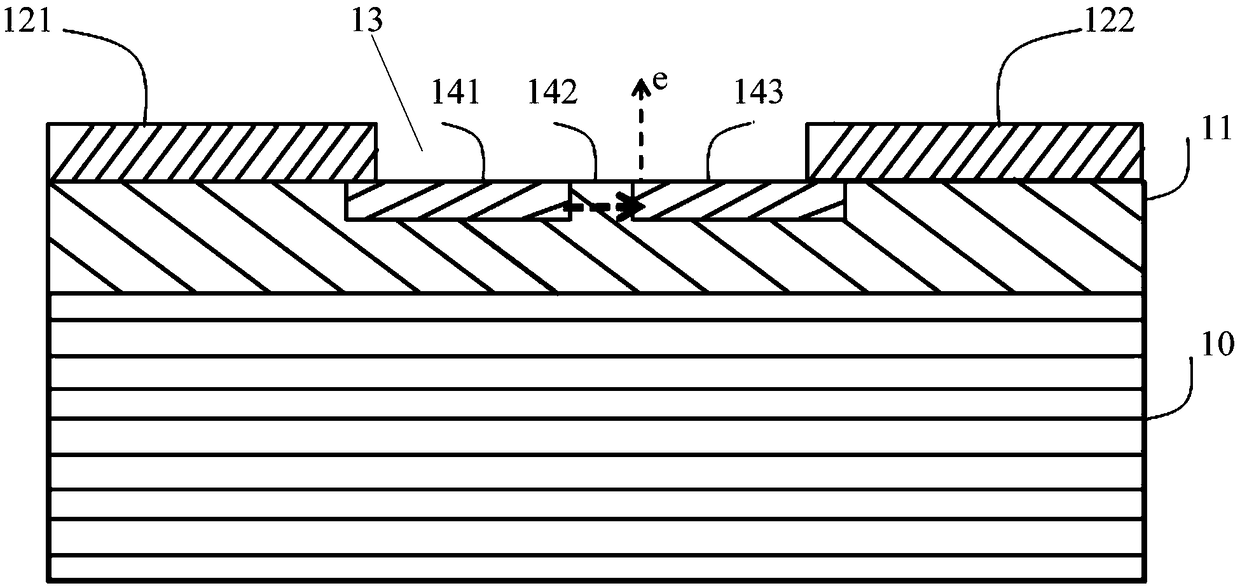
[0061] see figure 1 and figure 2 , figure 1 It is a schematic diagram of the three-dimensional structure of an on-chip micro-electron source provided in Embodiment 1 of the present application, figure 2 for the on-chip miniature electron source along the figure 1 The schematic diagram of the cross-sectional structure of the dotted line A-A'.

[0062] An on-chip miniature electron source comprising:

[0063] Heat conduction layer 10;

[0064] An insulating layer 11 located on the heat conducting layer 10, wherein the insulating layer 11 is made of a resistive material, and a through hole 111 is arranged on it;

[0065] An electrode pair located on the insulating layer 11, the electrode pair includes a first electrode 121 and a second electrode 122, and the second electrode 122 is in contact with the heat conducting layer 10 through the through hole 111;

[0066] Wherein, there is a gap 13 between the first electrode 121 and the second electrode 122 ; a tunnel junction 1...

Embodiment 2

[0108] see Figure 7 and Figure 8 , Figure 7 It is a schematic diagram of the three-dimensional structure of an on-chip micro-electron source provided in Embodiment 2 of the present application, Figure 8 for the on-chip miniature electron source along the Figure 7 The schematic diagram of the cross-sectional structure of B-B' in the middle.

[0109] An on-chip miniature electron source comprising:

[0110] heat conducting layer 70;

[0111] An insulating layer 71 located on the heat conducting layer 70, wherein the insulating layer 71 is made of a resistive material, and a plurality of through holes 711 are arranged on it;

[0112] A plurality of electrode pairs located on the insulating layer 71, each electrode pair includes a first electrode 721 and a second electrode 722, wherein each second electrode 722 corresponds to a through hole 711, and each second electrode 722 communicates with the through hole The heat conduction layer 70 is contacted and connected; the ...

Embodiment 3

[0151] It should be noted that the on-chip micro-electron source provided by the embodiment of the present application can be improved on the basis of the first or second embodiment above. As an example, the embodiment of the present application is obtained by improving the second embodiment.

[0152] see Figure 11 and Figure 12 , Figure 11 It is a schematic diagram of the three-dimensional structure of another on-chip micro-electron source provided in Embodiment 3 of the present application, Figure 12 for the on-chip miniature electron source along the Figure 11 The schematic diagram of the cross-sectional structure of C-C'.

[0153] In addition to all the components in Embodiment 2, the on-chip micro-electron source provided in this embodiment may also include:

[0154] Lead out electrode 110;

[0155] Wherein, the lead-out electrode 110 includes: a lead-out electrode layer 1101 and an insulating support structure 1102 located on one side of the lead-out electrode ...


PUM


Abstract

The invention discloses an on-chip micro electron source and a manufacturing method thereof. The on-chip micro electron source is provided with a heat conducting layer, and at least one electrode in the same pair of electrodes is connected with the heat conducting layer via a through hole of an insulating layer, so that heat generated by the on-chip micro electron source can be dissipated throughthe electrode and the heat conducting layer, and thus the heat dissipation ability of the on-chip electron source is significantly improved. Therefore, the on-chip micro electron source can integratemultiple single electron sources on the same substrate so as to form an electron source integration array with a high integration level, so that the on-chip electron source is enabled to have high overall emission current, and more application requirements are met. For example, the on-chip micro electron source provided by the invention can be widely applied to various electronic devices involvingan electron source such as X-ray tubs, microwave tubes and flat-panel displays.

Description

technical field [0001] The present application relates to the field of electronic science and technology, in particular to an on-chip micro-electronic source and a manufacturing method thereof. Background technique [0002] Vacuum electronic devices (such as X-ray tubes, microwave tubes, cathode ray tubes, etc.) are widely used in important fields such as aerospace, medical health, and scientific research, but they still face problems such as large volume, high power consumption, and difficulty in integration. Solving these problems One approach is to realize miniaturized on-chip vacuum electronics. The electron source is an essential key element of all vacuum electronic devices, providing the latter with the free electron beam necessary for its operation. At present, the miniaturization and on-chip electron source is one of the main bottlenecks limiting the miniaturization and on-chip vacuum electronic devices. Therefore, a high-performance on-chip miniature electron sourc...

Claims


Application Information

Patent Timeline
Patent Type & Authority Applications(China)
IPC IPC(8): H01J3/02H01J9/00
CPCH01J3/026H01J9/00
Inventor 魏贤龙杨威
Owner PEKING UNIV
Why Eureka
Try Eureka