Array substrate and preparation method thereof, and display panel

A technology of array substrates and thin film transistors, which is applied in photo-plate-making process coating equipment, photomechanical equipment, photo-plate-making process exposure devices, etc., and can solve problems such as poor contact between the source electrode and the metal light-shielding layer

Active Publication Date: 2019-02-01
BOE TECH GRP CO LTD
View PDF3 Cites 44 Cited by
  • Summary
  • Abstract
  • Description
  • Claims
  • Application Information

AI Technical Summary

Problems solved by technology

[0003] Embodiments of the present invention provide an array substrate and its preparation method, and a display...

Method used


Image

  • Array substrate and preparation method thereof, and display panel
  • Array substrate and preparation method thereof, and display panel
  • Array substrate and preparation method thereof, and display panel

Examples


Embodiment Construction

[0046] The following will clearly and completely describe the technical solutions in the embodiments of the present invention with reference to the accompanying drawings in the embodiments of the present invention. Obviously, the described embodiments are only some, not all, embodiments of the present invention. Based on the embodiments of the present invention, all other embodiments obtained by persons of ordinary skill in the art without making creative efforts belong to the protection scope of the present invention.

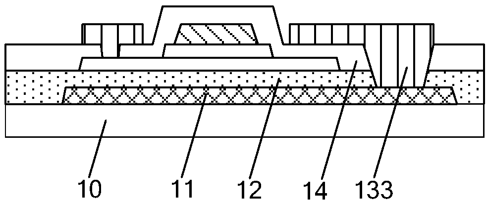
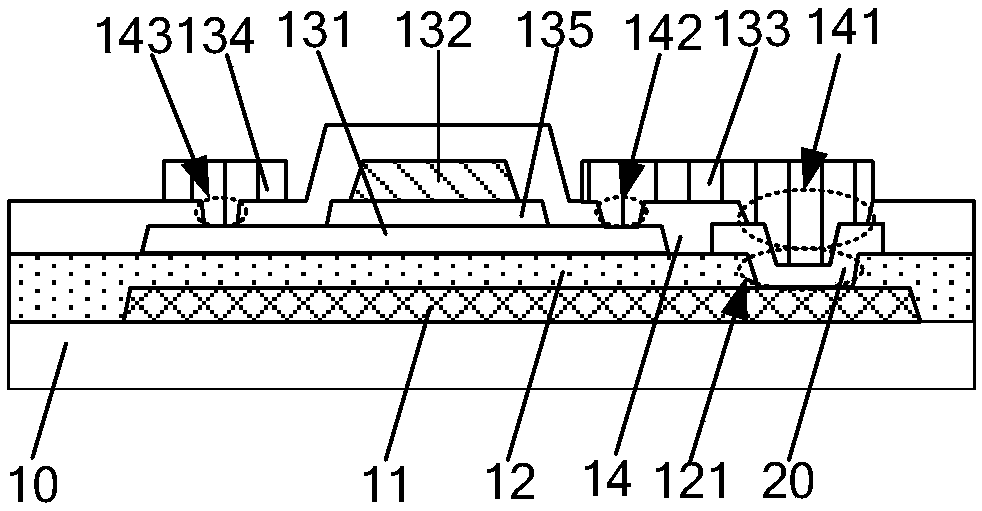
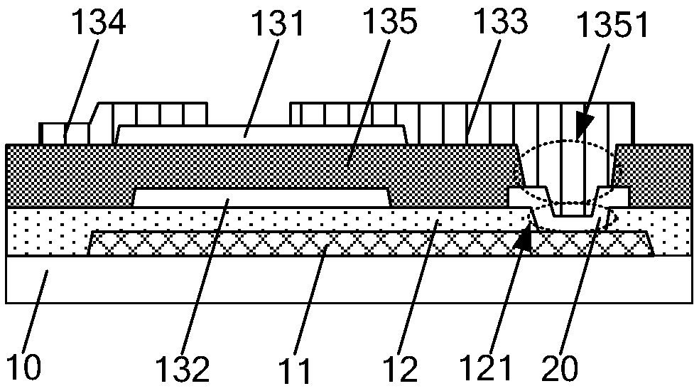
[0047] An embodiment of the present invention provides an array substrate, such as figure 2 and image 3 As shown, including a substrate 10, a metal light-shielding layer 11, a buffer layer 12, and a thin film transistor disposed on the substrate 10 in sequence, the thin film transistor includes a gate 132, an active layer 131, and a source 133 and a drain 134; The buffer layer 12 includes a first via hole 121 exposing the metal light shielding layer 11 ; th...


PUM


Abstract

The embodiment of the invention provides an array substrate and a preparation method thereof, and a display panel, and relates to the technical field of display. The problem can be solved that the contact of a source and a metal shielding layer is bad. The array substrate comprises a substrate, a metal shielding layer and a buffer layer which are arranged on the substrate in order and a thin filmtransistor. The thin film transistor comprises a gate, an active layer, a source and a drain; the buffer layer comprises a first via hole, and the via hole is exposed out of the metal shielding layer;and the source is electrically connected with the metal shielding layer through a conductive structure arranged in the via hole.

Description

technical field [0001] The present invention relates to the field of display technology, in particular to an array substrate, a preparation method thereof, and a display panel. Background technique [0002] Such as figure 1 As shown, the array substrate includes a metal light-shielding layer 11 and a buffer layer 12 located between the substrate 10 and the thin film transistor and sequentially disposed on the substrate 10 . In order to achieve better stability of oxide properties, the material of the buffer layer 12 is pure silicon oxide, and the thickness of the buffer layer 12 is relatively large. When dry etching is used to form the pattern of the buffer layer 12 and the interlayer insulating layer 14, in order to ensure that the etching is complete, a large amount of overetching is required, that is, the metal light-shielding layer located on the side of the buffer layer 12 close to the substrate 10 11 will also be etched, wherein, the greater the sum of the thicknesse...

Claims


Application Information

Patent Timeline
IPC IPC(8): H01L27/12H01L21/77H01L27/32
CPCH01L27/1214H01L27/1259H10K59/131H10K71/00H01L29/78633H01L27/124G02F1/136209G02F1/136231G02F1/13606G02F1/13685H10K59/126G02F1/1368G03F7/16G03F7/20G03F7/2024G03F7/26H01L27/1225H01L27/1255H01L27/127H01L27/1288H01L29/7869H10K59/1201H10K59/1213H10K59/1216
Inventor 方金钢丁录科刘军程磊磊
Owner BOE TECH GRP CO LTD
Why Eureka
Try Eureka