Camera module and camera device

A camera module and semiconductor technology, applied in measurement devices, radiation control devices, image communication, etc., can solve problems such as crystal defects, and achieve the effects of high resolution, high resolution, and low weight

Active Publication Date: 2020-08-04
雫石诚
View PDF6 Cites 0 Cited by
  • Summary
  • Abstract
  • Description
  • Claims
  • Application Information

AI Technical Summary

Problems solved by technology

Therefore, the peripheral portion or the side wall portion of the surface of the imaging element is mechanically damaged or thermally damaged by the dicing process, resulting in crystal defects, and is exposed to contamination from external heavy metals, reactive chemical substances, etc.
Therefore, there are still unresolved technical problems in the imaging element that uses the side surface of the substrate as the light receiving part like this.

Method used


Image

  • Camera module and camera device
  • Camera module and camera device
  • Camera module and camera device

Examples


Embodiment Construction

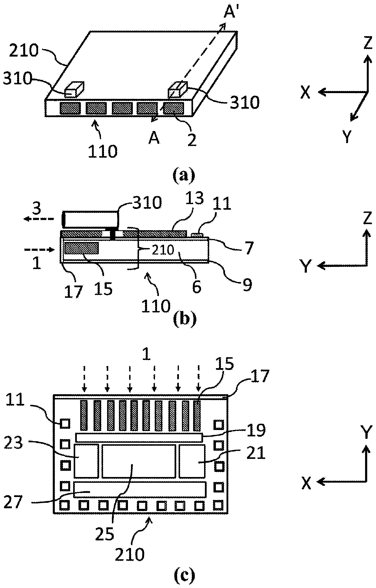
[0075] A camera module according to a first embodiment of the present invention will be described. figure 1 (a) shows a perspective view and three-dimensional coordinate axes of the camera module 110 . In order to describe the camera module 110 and its components, three-dimensional coordinate axes are defined. The surface of the semiconductor substrate on which the integrated circuit is formed is defined as the X-Y plane, and the direction perpendicular to the surface of the semiconductor substrate, that is, the thickness direction of the semiconductor substrate is defined as the Z-axis. In the semiconductor substrate, for example, a side surface (X-Z plane) of a silicon substrate is provided with a plurality of light-receiving windows 2 , which represent portions that receive incident light. As will be described below, the portion corresponding to the light receiving window 2 is the end of the photoelectric conversion region extending in the Y-axis direction in the semicondu...


PUM

PropertyMeasurementUnit
thicknessaaaaaaaaaa
spectral sensitivityaaaaaaaaaa

Abstract

The present invention improves the resolution of space, time, and energy in imaging devices such as optical mapping devices and optical CT devices, and greatly improves the accuracy of image diagnosis by reducing the size and weight of imaging devices, thereby realizing early detection of diseases and medical expenses. reduction. The present invention provides an imaging device of an imaging module. The imaging module is a semiconductor imaging element that uses the side surface of the semiconductor substrate in the direction perpendicular to the surface of the semiconductor substrate on which the integrated circuit is formed as a light-receiving surface. On the substrate surface, one or more light source sections are arranged such that the light emitting direction from the light source section coincides with the normal direction of the side surface of the substrate.

Description

technical field [0001] The present invention relates to an imaging module that is excellent in energy, space, and time resolution, and realizes high sensitivity, small size, light weight, and low power consumption, and an imaging device using the imaging module. Background technique [0002] Conventionally, an optical CT (computed tomography) apparatus using near-infrared light is disclosed (Patent Document 1). However, since it is necessary to arrange a plurality of detectors radially or to rotate the light source around the subject, sufficient spatial resolution cannot be obtained, and it is difficult to reduce the size and weight of the device. Similarly, a mammography apparatus using near-infrared light is also disclosed (Patent Document 2), but since there are restrictions on the arrangement of detectors and light sources conforming to the shape of the subject and the number of detectors is also limited, It is difficult to find small lesions in the early stage or withi...

Claims


Application Information

Patent Timeline
Patent Type & Authority Patents(China)
IPC IPC(8): H01L27/146H04N5/369A61B1/00A61B1/04A61B8/00A61B10/00G01N21/17H01L27/144H01L27/15H01L31/02H04N5/33
CPCA61B1/00A61B8/00A61B10/00G01N21/17H01L31/02H01L27/144H01L27/146H01L27/15H04N5/33A61B1/044A61B1/046A61B1/043H04N25/70
Inventor 雫石诚
Owner 雫石诚
Why Eureka
Try Eureka