Supercharge Your Innovation With Domain-Expert AI Agents!

A touch sensor and a touch display panel

A technology of touch sensing and substrate, which is applied in the fields of instruments, computing, electrical digital data processing, etc., and can solve problems such as poor etching of metal grids, low yield rate of touch sensors, and discoloration

Active Publication Date: 2021-12-17
TRULY OPTO ELECTRONICS
View PDF9 Cites 0 Cited by
  • Summary
  • Abstract
  • Description
  • Claims
  • Application Information

AI Technical Summary

Problems solved by technology

However, in the prior art, the metal grid obtained by etching usually has bad conditions such as poor etching, jagged lines, and different colors, which make the touch sensor have a low yield rate.

Method used


Image

  • A touch sensor and a touch display panel
  • A touch sensor and a touch display panel
  • A touch sensor and a touch display panel

Examples


Embodiment Construction

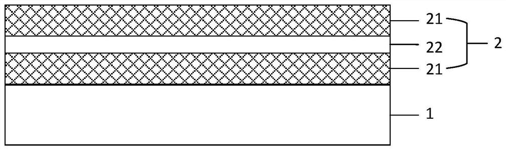
[0026] The core of the present invention is to provide a touch sensor. In the prior art, the conductive wire constituting the conductive grid layer is typically a three-layer structure having a sandwich type, wherein the conductive layer is located in the middle, and is a black layer on both sides. In the prior art, the conductive mesh layer is prepared in one etching process in one etching process. In the etching process, a case where the blacking layer and the conductive layer have inconsistent amount, for example, if the side etching amount of the black layer is larger than the side etching of the conductive layer, the conductive layer is easily exposed to generate a different color. Situation; if the side etching of the black layer is significantly smaller than the side etching of the conductive layer, when the wire width of the conductive mesh is guaranteed, the conductive wire break, the ablation, and the line saw to tease, that is, when When the surface of the blacking laye...


PUM

PropertyMeasurementUnit
thicknessaaaaaaaaaa
thicknessaaaaaaaaaa

Abstract

The invention discloses a touch sensor, which includes a conductive grid layer in a sandwich structure, the conductive grid layer includes a first blackened layer facing the substrate, a second blackened layer facing away from the substrate, The conductive layer between the blackened layer and the second blackened layer. Wherein the first blackened layer is tantalum with a mass fraction of 3%-5% added to molybdenum oxide; the second blackened layer is tantalum with a mass fraction of 5%-8% added to molybdenum oxide; the conductive layer is copper Tantalum is added with a mass fraction of 15%-20%. When preparing the conductive grid layer, the above-mentioned film layers will be etched sequentially from the direction of the second blackened layer; doping the above-mentioned film layers with different concentrations of tantalum can ensure that the first blackened layer, the second blackened layer, and the conductive layer have basically the same amount of undercut, so that the touch sensor can have a higher yield rate. The embodiment of the present invention also provides a touch display panel, which also has the above beneficial effects.

Description

Technical field [0001] The present invention relates to the field of touch technologies, and more particularly to a touch sensor and a touch display panel. Background technique [0002] With the continuous advancement in technology in recent years, the development of the product industry has made great progress in the development of the product industry, the touch sensor has made great progress in terms of size or performance. Correspondingly, the user has a higher requirement for the details and appearance of the touch product. [0003] In recent years, the Metal Mesh-type touch sensor has been more and more attention in the market with its low resistance, integration, and simple advantages. At this stage, the conductive layer mainly in the metal mesh is usually copper, aluminum, and the like as the main material. However, the reflectance of the conductive layer of the metal is high, which will make the line of the metal mesh are obvious. In the prior art, in order to reduce the...

Claims


Application Information

Patent Timeline
Patent Type & Authority Patents(China)
IPC IPC(8): G06F3/041
CPCG06F3/0412
Inventor 刘威吴德生
Owner TRULY OPTO ELECTRONICS
Features
  • R&D
  • Intellectual Property
  • Life Sciences
  • Materials
  • Tech Scout
  • Unparalleled Data Quality
  • Higher Quality Content
  • 60% Fewer Hallucinations
Learn More