A defect detection device and method for a large-aperture plane mirror based on line scanning and ring-band splicing

A defect detection and line scanning technology, applied in the field of optical detection, can solve the problems of large imaging distortion of sub-aperture data, distortion correction position correction, large amount of intermediate data, etc., and achieve simple and accurate position error correction, small calculation amount, and data amount. small effect

Active Publication Date: 2021-06-18
INST OF OPTICS & ELECTRONICS - CHINESE ACAD OF SCI
View PDF0 Cites 0 Cited by
  • Summary
  • Abstract
  • Description
  • Claims
  • Application Information

AI Technical Summary

Problems solved by technology

At the beginning of the 21st century, the American QED company produced the SSI automatic splicing interferometer to realize the automatic splicing measurement of optical components, but the detection accuracy is low, and it is only used as a process detection instrument in high-precision lens processing
At present, the existing surface flaw detection device is mainly based on area array camera scanning. The disadvantages are that there are many sub-apertures, long detection time, large amount of intermediate data, large distortion of sub-aperture data imaging, and difficult distortion correction and position correction during splicing.

Method used


Image

  • A defect detection device and method for a large-aperture plane mirror based on line scanning and ring-band splicing
  • A defect detection device and method for a large-aperture plane mirror based on line scanning and ring-band splicing
  • A defect detection device and method for a large-aperture plane mirror based on line scanning and ring-band splicing

Examples


Embodiment Construction

[0039] The present invention will be further described below in conjunction with the accompanying drawings and specific embodiments.

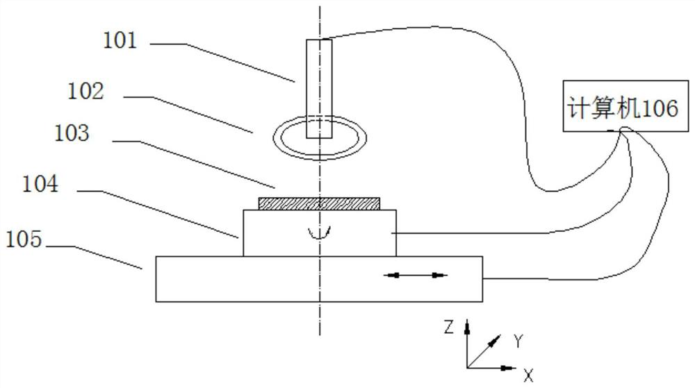
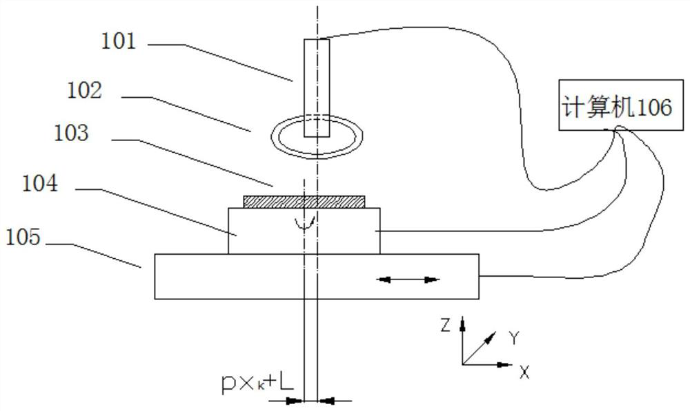
[0040] figure 1 It is a schematic diagram of a defect detection device for a large-diameter plane mirror based on line scanning and ring splicing of the present invention, including a line scanning detector 101, an annular illumination source 102, a plane mirror under test 103, a rotating table 104 around the Z axis, and The translation platform 105 of X axis, computer 106, the structural representation of its device is as figure 1 shown. The XYZ coordinate system is the coordinate system of the rotating stage 104 around the Z axis and the translation stage 105 along the X axis. Wherein, the rotating platform 104 around the Z axis realizes the rotation around the Z direction, and the translation platform 105 along the X axis realizes the translation along the X direction. The rotating platform 104 around the Z axis is placed on the translati...


PUM


Abstract

The invention discloses a defect detection device and method for a large-diameter plane mirror based on line scanning and ring belt splicing. platform, computer. By translating and rotating the measured plane mirror, the entire surface of the measured plane mirror can be detected by the scanning detector, and the defect situation of the whole measured plane mirror is obtained through the ring band splicing method. Among them, the method of line scanning and ring-band splicing reduces imaging distortion, the amount of intermediate data, the difficulty of distortion correction and splicing, and improves the detection speed and detection quality.

Description

technical field [0001] The invention belongs to the field of optical detection, and in particular relates to a defect detection device and method for a large-diameter flat mirror based on line scanning and ring splicing. Background technique [0002] The lithography lens is a complex optical system composed of dozens of lenses, some of which have large apertures, and it is difficult to develop corresponding standard lenses. Stitching measurement plans a mirror surface into multiple small sub-apertures, and measures each sub-aperture one by one, and then combines the surface shape of the sub-apertures into the surface shape of the entire mirror surface through an algorithm. At the beginning of the 21st century, the American QED company produced the SSI automatic splicing interferometer to realize the automatic splicing measurement of optical components, but the detection accuracy is low, and it is only used as a process detection instrument in high-precision lens processing. ...

Claims


Application Information

Patent Timeline
Patent Type & Authority Patents(China)
IPC IPC(8): G01N21/896G01M11/00
CPCG01M11/00G01N21/896G01N21/95G01N2021/8887G01N2021/9511D06H3/08G01N21/8983G02B26/105
Inventor 徐富超全海洋付韬韬胡小川侯溪李声
Owner INST OF OPTICS & ELECTRONICS - CHINESE ACAD OF SCI
Why Eureka
Try Eureka