Heterojunction solar cell based on n-type silicon wafer and manufacturing method thereof

A technology of a solar cell and a manufacturing method, which is applied in the field of solar cells, can solve the problems of complex process, expensive equipment, complicated manufacturing process and equipment, etc., and achieves the effect of increasing the light absorption area and simplifying the manufacturing process

Pending Publication Date: 2019-02-22
黄剑鸣
View PDF5 Cites 2 Cited by
  • Summary
  • Abstract
  • Description
  • Claims
  • Application Information

AI Technical Summary

Problems solved by technology

[0002] Heterojunction solar cell, referred to as HIT, is a silicon wafer solar cell with high conversion efficiency. The problems faced by this kind of solar cell are that the process is too complicated and the equipment is too expensive. Therefore, its commercial application value is greatly limited.
[0003] In the traditional manufacturing process, the silicon wafer is first chemically treated to passivate the surface and produce uneven suede, and then transferred to the plasma-enhanced chemical vapor deposition equipment to deposit the p-i and i-n layers of amorphous silicon to form a thin film. Then transfer to the magnetron sputtering equipment to coat ITO, and then print the grid line and use laser edge cleaning. The process and equipment are quite complicated.

Method used


Image

  • Heterojunction solar cell based on n-type silicon wafer and manufacturing method thereof
  • Heterojunction solar cell based on n-type silicon wafer and manufacturing method thereof

Examples


Embodiment 1

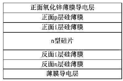
[0037] A heterojunction solar cell based on an n-type silicon wafer, comprising an n-type silicon wafer, an i-layer silicon thin film on the front side, a p-layer silicon thin film on the front side, an i-layer silicon thin film on the back side, an n-layer silicon thin film on the back side, and a zinc oxide thin film conductive layer on the front side and a thin film conductive layer, where:

[0038] The front side of the n-type silicon wafer is deposited with a front i-layer silicon film by plasma chemical vapor deposition PECVD method, and a front p-layer silicon film is deposited on the front i-layer silicon film by plasma chemical vapor deposition PECVD method, and a front p-layer silicon film is deposited on the front side i-layer silicon film The conductive layer of zinc oxide thin film on the upper side is deposited by chemical vapor deposition CVD method, and the i-layer silicon film on the reverse side is deposited by plasma chemical vapor deposition PECVD method on ...

Embodiment 2

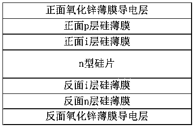
[0046] A heterojunction solar cell based on n-type silicon wafers, such as figure 2 , including an n-type silicon wafer, an i-layer silicon film on the front side, a p-layer silicon film on the front side, an i-layer silicon film on the back side, an n-layer silicon film on the back side, a conductive layer of a transparent zinc oxide film on the front side and a conductive layer of a zinc oxide thin film on the back side, wherein:

[0047] The front side of the n-type silicon wafer is deposited with a front i-layer silicon film by plasma chemical vapor deposition PECVD method, and a front p-layer silicon film is deposited on the front i-layer silicon film by plasma chemical vapor deposition PECVD method, and a front p-layer silicon film is deposited on the front side i-layer silicon film The conductive layer of zinc oxide thin film on the upper side is deposited by chemical vapor deposition CVD method, and the i-layer silicon film on the reverse side is deposited by plasma ch...


PUM


Abstract

The invention discloses a heterojunction solar cell based on an n-type silicon wafer, comprising an n-type silicon wafer, a front-side i-layer silicon film, a front-side p-layer silicon film, a reverse-side i-layer silicon film, a reverse-side n-layer silicon film, a front-side film conductive layer and a reverse-side film conductive layer, wherein at least one of the front-side film conductive layer and the reverse-side film conductive layer is a zinc oxide film conductive layer; the front-side i-layer silicon film, the front-side p-layer silicon film, and the front-side film conductive layerare successively deposited on the front side of the n-type silicon wafer; and the reverse-side i-layer silicon film, the reverse-side n-layer silicon film and the reverse-side film conductive layer are successively deposited on the reverse side of the n-type silicon wafer. The manufacturing method of the heterojunction solar cell of the invention is a completely dry process, clean and hygienic, can achieve fully automated production to reduce manpower, is low in the vacuum coating process cost, and greatly improves the market application value of the heterojunction solar cell.

Description

technical field [0001] The invention relates to the field of solar cells, and more specifically, to a heterojunction solar cell based on n-type silicon wafers and a manufacturing method thereof. Background technique [0002] Heterojunction solar cell, referred to as HIT, is a silicon wafer solar cell with high conversion efficiency. The problem faced by this kind of solar cell is that the process is too complicated and the equipment is too expensive. Therefore, its commercial application value is greatly limited. [0003] In the traditional manufacturing process, the silicon wafer is first chemically treated to passivate the surface and produce uneven suede, and then transferred to the plasma-enhanced chemical vapor deposition equipment to deposit the p-i and i-n layers of amorphous silicon to form a thin film. It is then transferred to the magnetron sputtering equipment to coat ITO, and then the grid lines are printed and the edges are cleaned with lasers. The process and e...

Claims


Application Information

Patent Timeline
Patent Type & Authority Applications(China)
IPC IPC(8): H01L31/0224H01L31/0747H01L31/18
CPCH01L31/022425H01L31/022483H01L31/0747H01L31/1804H01L31/1884Y02E10/547Y02P70/50
Inventor 范继良
Owner 黄剑鸣
Why Eureka
Try Eureka