Broad-band high-performance photodetector based on palladium selenide thin film/silicon cone wrapping structure heterojunction and its manufacturing method

A photodetector and wide-band technology, applied in circuits, electrical components, nano-optics, etc., can solve the problems of limiting graphene applications, high electron mobility, high preparation costs, etc., to achieve broadened photoelectric performance, large light absorption area, The effect of stable performance

Active Publication Date: 2021-11-30
HEFEI UNIV OF TECH
View PDF0 Cites 0 Cited by
  • Summary
  • Abstract
  • Description
  • Claims
  • Application Information

AI Technical Summary

Problems solved by technology

In recent years, with the emergence of graphene, a widespread research boom has been set off, and it has been used in photodetectors because of its high electron mobility, but its no band gap, low absorbance and high preparation cost limit The further application of graphene
Then appeared black scale, also known as phosphorene, which has a narrow band gap and relatively high electron mobility, and is used in the research of infrared devices, but phosphorene has a fatal flaw—poor stability

Method used


Image

  • Broad-band high-performance photodetector based on palladium selenide thin film/silicon cone wrapping structure heterojunction and its manufacturing method
  • Broad-band high-performance photodetector based on palladium selenide thin film/silicon cone wrapping structure heterojunction and its manufacturing method
  • Broad-band high-performance photodetector based on palladium selenide thin film/silicon cone wrapping structure heterojunction and its manufacturing method

Examples


Embodiment 1

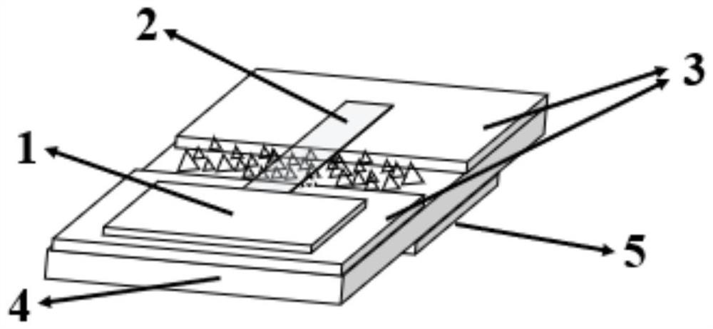
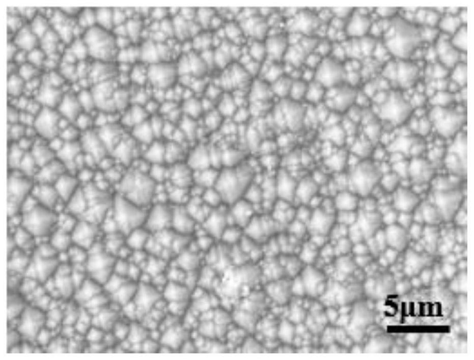
[0031] Such as figure 1 As shown, the photodetector of the present embodiment is based on an n-type lightly doped silicon wafer with a silicon oxide layer (a 300nm thick silicon oxide 3 is arranged on a 500 micron thick n-type lightly doped silicon 4, lightly doped silicon resistors The ratio is 1~5Ω*cm); in the first area of ​​the substrate (1mm*5mm), the upper silicon oxide is etched away by acid method to form a window exposing the lower silicon, and then the silicon in the window is etched by alkali etching It is a silicon cone structure; in the second area of ​​the substrate (1mm*5mm, perpendicular to the first area, forming a cross structure) by first evaporating a metal palladium film and then selenizing the metal palladium film, a PdSe 2 Film 2; the second area and the first area have an overlapping area of ​​1 mm*1 mm; an In / Ga alloy electrode (about 300 nm in thickness) forming an ohmic contact with the silicon cone structure is provided on the lower surface of the s...


PUM

PropertyMeasurementUnit
thicknessaaaaaaaaaa
thicknessaaaaaaaaaa
thicknessaaaaaaaaaa

Abstract

The invention discloses a wide-band high-performance photodetector based on a palladium selenide thin film / silicon cone wrapped structure heterojunction and a preparation method thereof. The silicon cone is firstly etched on an n-type lightly doped silicon wafer with a silicon oxide layer. structure, and then wrap PdSe outside the silicon cone structure 2 film, so that the two form a heterojunction. The photoelectric detector of the invention has simple device preparation process, stable and good performance, and opens up new prospects for the application of transition group metal selenide materials in photoelectric detectors.

Description

technical field [0001] The invention belongs to the field of semiconductor photodetectors, and in particular relates to a wide-band high-performance photodetector based on a palladium selenide film / silicon cone wrapping structure heterojunction and a manufacturing method thereof. Background technique [0002] Photodetectors are widely used in optical communication, imaging, and biosensing because they can convert optical signals into electrical output signals. In recent years, with the emergence of graphene, a widespread research boom has been set off, and it has been used in photodetectors because of its high electron mobility, but its no band gap, low absorbance and high preparation cost limit further applications of graphene. Then appeared black scale, also known as phosphorene, which has a narrow band gap and relatively high electron mobility, and has been used in the research of infrared devices, but phosphorene has a fatal flaw—poor stability. More and more researche...

Claims


Application Information

Patent Timeline
Patent Type & Authority Patents(China)
IPC IPC(8): H01L31/109H01L31/0336H01L31/0392H01L31/18B82Y20/00
CPCB82Y20/00H01L31/0336H01L31/0392H01L31/109H01L31/18Y02P70/50
Inventor 梁凤霞赵兴远范荣誉罗林保蒋静静
Owner HEFEI UNIV OF TECH
Why Eureka
Try Eureka