A kind of solar cell structure of Ⅲ-ⅴ semiconductor and its manufacturing method

A technology of solar cells and semiconductors, applied in the field of solar cells, can solve the problems that photoelectric conversion efficiency cannot be further improved, solar cells have no protection measures, and chip costs are high, so as to effectively absorb light energy, reduce total costs, and increase service life. Effect

Inactive Publication Date: 2018-02-23
YANBIAN UNIV
View PDF5 Cites 0 Cited by
  • Summary
  • Abstract
  • Description
  • Claims
  • Application Information

AI Technical Summary

Problems solved by technology

Although Ⅲ-Ⅴ solar cells do not need to use silicon crystals, the cost of chips is still relatively high, and the current solar cells do not have corresponding protection measures, so that their lifespan is still not long; and most of the solar cells are flat structure, so that part of the sunlight reflection causes losses and other factors, resulting in the inability to further improve the photoelectric conversion efficiency

Method used


Image

  • A kind of solar cell structure of Ⅲ-ⅴ semiconductor and its manufacturing method
  • A kind of solar cell structure of Ⅲ-ⅴ semiconductor and its manufacturing method

Examples


Embodiment Construction

[0023] The following will clearly and completely describe the technical solutions in the embodiments of the present invention with reference to the accompanying drawings in the embodiments of the present invention. Obviously, the described embodiments are only some, not all, embodiments of the present invention. Based on the embodiments of the present invention, all other embodiments obtained by persons of ordinary skill in the art without making creative efforts belong to the protection scope of the present invention.

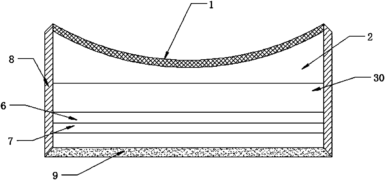
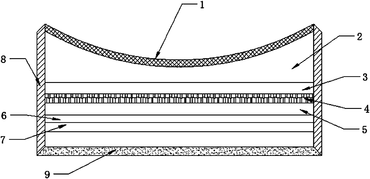
[0024] see Figure 1~2 , in an embodiment of the present invention, a solar cell structure of III-V semiconductors, including a protective shell 8 and a transparent substrate 7 disposed in the protective shell 8, an amorphous silicon layer 6, and a III-V polycrystalline semiconductor layer 30 , a transparent light guiding layer 2, a light absorbing layer 1, and a protective base plate 9, the transparent substrate 7 is arranged under the inside of the protectiv...


PUM


Abstract

The invention discloses an III-V family semiconductor solar energy cell structure and manufacturing method thereof, comprising a protection housing and the following layers arranged inside the protection housing in succession from the bottom to the top: a transparent substrate, an amorphous silicon layer, an III-V family polycrystalline semiconductor layer, a transparent light transmission layer and a light absorption layer. The bottom end of the protection layer is flexibly provided with a protection bottom plate. The light absorption layer is designed into a recessed arc shape and agrees with the concave groove on the transparent light transmission layer; the surface and the inner part of the transparent light transmission layer are provided with a plurality of micro-holes so that incoming light rays could be guided into the III-V family polycrystalline semiconductor layer horizontally. In the invention, an arc shaped light absorption layer, a transparent light transmission layer and a transparent substrate are used in the structure, which not only extends the service life of the structure and reduces the overall cost, but also increases the light absorption size, effectively absorbs light energy and raises the conversion efficiency of the solar energy cell to the light.

Description

technical field [0001] The invention relates to the field of solar cells, in particular to a III-V group semiconductor solar cell structure and a manufacturing method thereof. Background technique [0002] From the 20th century to the 21st century, with the progress of people's life, the demand for energy is getting higher and higher. However, due to the limited resources available on the earth, in order to avoid the exhaustion of resources, the solar energy industry came into being. Solar energy is a kind of A green and sustainable energy, the development of solar cells can store light energy and make use of it. A solar cell is a semiconductor that absorbs light or photons, and electrons are excited and transition, and the excited electrons drive the circuit to form a battery semiconductor. Various solar cell materials currently used include semiconductor types such as monocrystalline silicon, polycrystalline silicon, and amorphous silicon, or materials linked by elements ...

Claims


Application Information

Patent Timeline
Patent Type & Authority Patents(China)
IPC IPC(8): H01L31/054H01L31/077H01L31/18
CPCH01L31/054H01L31/077H01L31/184Y02E10/52Y02E10/544Y02E10/546Y02P70/50
Inventor 吴宝嘉王俊盈赵晨谷雨时
Owner YANBIAN UNIV
Why Eureka
Try Eureka