Display device and preparation method thereof

A technology of display equipment and solution method, which is applied in semiconductor/solid-state device manufacturing, electrical components, electric solid-state devices, etc., and can solve problems such as short service life, inability to dissipate heat from devices in time, and low luminous efficiency of devices

Active Publication Date: 2019-02-26
TCL CORPORATION
View PDF4 Cites 4 Cited by
  • Summary
  • Abstract
  • Description
  • Claims
  • Application Information

AI Technical Summary

Problems solved by technology

[0005] The purpose of the present invention is to provide a display device and its preparation method, aiming to solve the problem that the existing light-emitting device cannot dissipate the heat of the device in time due to the sealed environment of the package, so that the device has low luminous efficiency and short service life The problem

Method used


Image

  • Display device and preparation method thereof
  • Display device and preparation method thereof
  • Display device and preparation method thereof

Examples


preparation example Construction

[0054] An embodiment of the present invention provides a method for manufacturing a display device, and the method includes the following steps:

[0055] Step S101: providing a substrate.

[0056] Step S102: forming a light emitting device on the substrate.

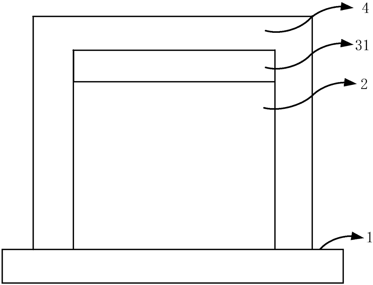
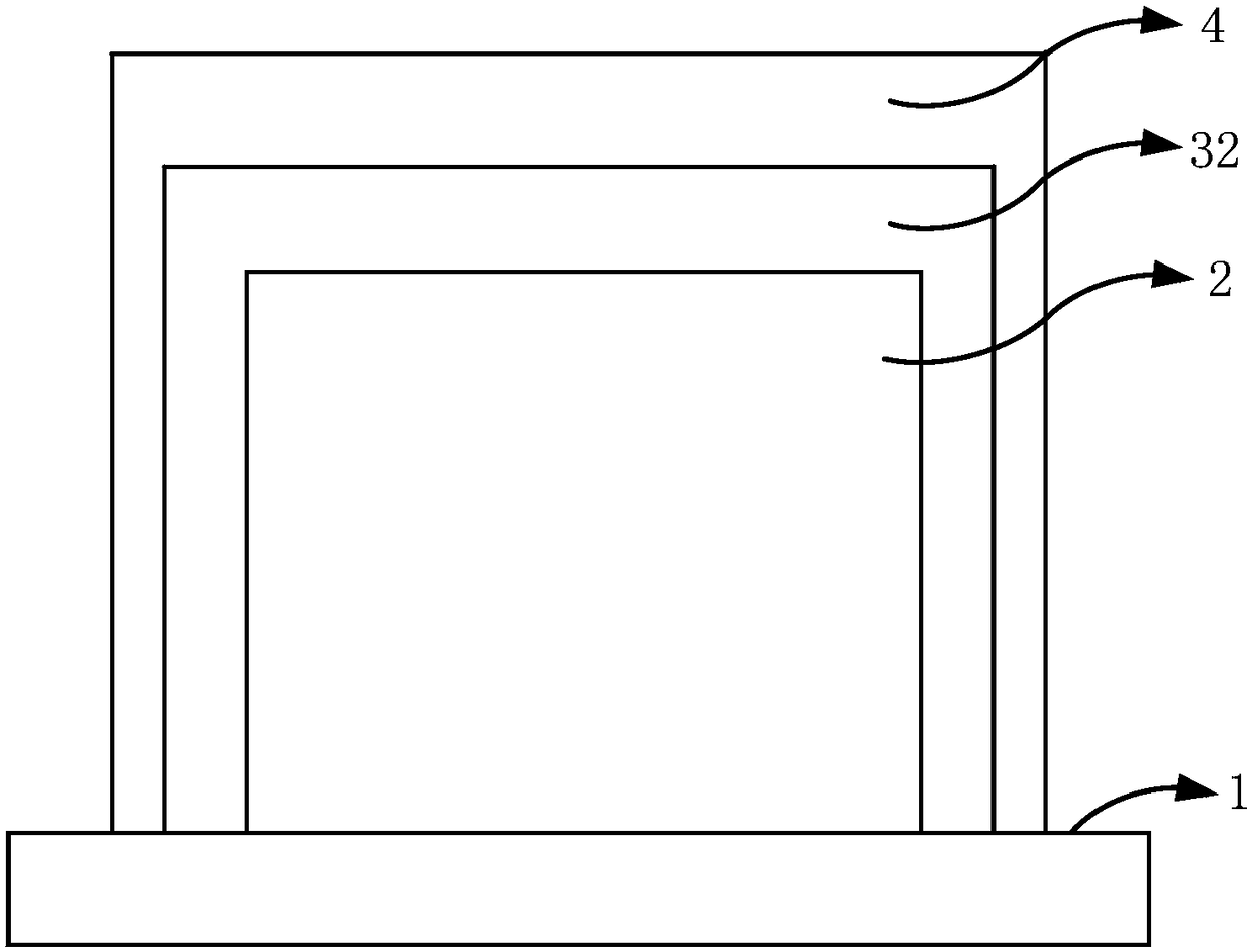
[0057] Step S103: disposing the first encapsulation layer on the bottom of the second encapsulation layer to form an encapsulation structure. The step of forming the first encapsulation layer includes: disposing a first metal nanoparticle / second metal nanowire layer on the second encapsulation layer, and disposing a carbon material layer on the first metal nanoparticle / second metal nanowire layer.

[0058] Step S104: Encapsulating the encapsulation structure on the substrate and the light emitting device to cover the light emitting device, wherein the first encapsulation layer is disposed between the light emitting device and the second encapsulation layer.

[0059] In the embodiment of the present invention, the releva...


PUM

PropertyMeasurementUnit
thicknessaaaaaaaaaa
thicknessaaaaaaaaaa
thicknessaaaaaaaaaa

Abstract

The present invention belongs to the field of display devices, and provides a display device and a preparation method thereof. The display device comprises a substrate, a light-emitting device, a first package layer and a second package layer, the first package layer comprises a carbon material layer and first metal nanoparticles/second metal nanowire layer. The carbon material layer is high in light transmission and good in thermal conductivity can effectively absorb the heat emitted by the device; the first metal nanoparticles and the second metal nanowire layer have good electrical conductivity, the first metal nanoparticles are diffused and attach to the surface of the second metal nanowire to allow the surface of the second metal nanowire layer to be rough to block the light refraction so that the first metal nanoparticles and the second metal nanowire layer have high light transmission and heat stability and can ensue the continuous stability of the first package layer light transmission thermal conductivity; through combination of the advantages of the two, the first package layer can ensure the continuous stability of the light transmission thermal conductivity of the device while timely emit the heat emitted by the device so as to improve the device life.

Description

technical field [0001] The invention belongs to the field of display devices, in particular to a display device and a preparation method thereof. Background technique [0002] Quantum dots (Quantum dots, QDs) have the characteristics of tunable luminescence, narrow luminescence line width, high photoluminescence efficiency and thermal stability, so the quantum dot light-emitting diode (QLED) with quantum dots as the light-emitting layer is very Potential next-generation display and solid-state lighting sources. [0003] Quantum dot light-emitting diodes have received extensive attention and research in the fields of lighting and display in recent years due to their advantages such as high brightness, low power consumption, wide color gamut, and easy processing. However, due to the poor waterproof and oxygen performance of the existing QLED devices, water and oxygen in the air can easily penetrate into the QLED devices and affect the performance of the devices. Therefore, t...

Claims


Application Information

Patent Timeline
Patent Type & Authority Applications(China)
IPC IPC(8): H01L51/50H01L51/52H01L51/56H01L27/32
CPCH10K59/00H10K50/115H10K50/84H10K71/00
Inventor 刘佳曹蔚然梁柱荣
Owner TCL CORPORATION
Why Eureka
Try Eureka