Optimization method of random vibration stress and return loss of chip package solder joints

A return loss and random vibration technology, applied in design optimization/simulation, special data processing applications, instruments, etc., can solve the problems of not taking into account the vibration analysis and signal integrity of solder joints, so as to improve reliability and signal integrity , random vibration stress and callback loss reduction, and the effect of inhibiting premature convergence

Active Publication Date: 2019-03-01
GUILIN UNIV OF ELECTRONIC TECH
View PDF14 Cites 14 Cited by
  • Summary
  • Abstract
  • Description
  • Claims
  • Application Information

AI Technical Summary

Problems solved by technology

[0010] In the above two documents, the influence of the size parameters of solder joints on the return loss of solder joints was studied, but the existing research results reflect that domestic and foreign scholars are limited to unilateral vibration analysis or unilateral vibration analysis of solder joints. The study of signal integrity does not take into account the vibration analysis an

Method used


Image

  • Optimization method of random vibration stress and return loss of chip package solder joints
  • Optimization method of random vibration stress and return loss of chip package solder joints
  • Optimization method of random vibration stress and return loss of chip package solder joints

Examples


Embodiment Construction

[0064] The present invention will be further described below in conjunction with the accompanying drawings and embodiments.

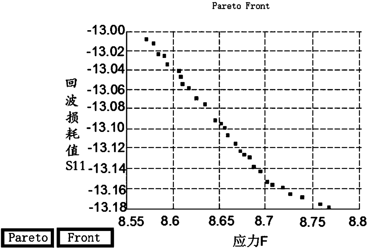
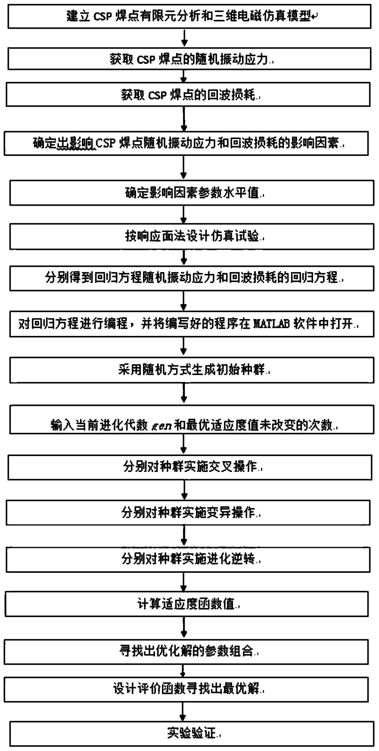
[0065] Such as Figure 1 to Figure 14 As shown, the method for optimizing random vibration stress and return loss of chip packaging solder joints according to the present invention comprises the following steps:

[0066] Step 1: Establish a CSP solder joint finite element analysis model and a three-dimensional electromagnetic simulation model: the model is an organic substrate 1, a solder joint 2 and a printed circuit board 3 stacked sequentially from top to bottom;

[0067] Step 2: Obtain the random vibration stress of the CSP solder joint: impose constraints on the model built in step 1), conduct analysis under random vibration loading conditions, and then use ANSYS software to simulate and analyze the model to obtain the stress distribution of the CSP solder joint;

[0068] Step 3: Obtain the return loss of the CSP solder joint: apply wave port exci...


PUM


Abstract

The invention discloses an optimization method for improving random vibration stress and echo loss of chip package solder joints by unilaterally performing vibration analysis research or unilateral echo loss research. CSP solder joint models are established in ANSYS and HFSS software, the finite element analysis model and three-dimensional electromagnetic simulation analysis of the model are carried out, Response surface method is used to design the horizontal combination of multi-group solder joint morphology parameters and to model for simulation calculation, and the response surface methodis used to calculate the stress value, the relationship between the return loss and the shape parameters of CSP solder joints is fitted, The initial population generation, crossover, mutation and evolutionary inversion were performed on the fitting function respectively, and the two populations were evaluated and updated as a whole. The local catastrophe is performed on the population if the conditions were satisfied, and the random vibration stress value and echo loss value of CSP solder joints were obtained while the parameter level combination is reduced. This method can be used to guide the design of structural parameters which take into account the random vibration stress and return loss of CSP solder joints.

Description

technical field [0001] The invention relates to the technical field of microelectronic packaging reliability and signal integrity, in particular to a method for optimizing random vibration stress and return loss of chip packaging solder joints based on response surface and genetic algorithm. Background technique [0002] With the rapid development of automotive electronic devices and other consumer electronics products, microelectronic packaging technology is facing the challenges and opportunities of "miniaturization, multi-function, high integration and low cost". Chip Scale Package (CSP) technology developed on the basis of QFP (Quad Flat Package) and TQFP (Plastic Quad Flat Package) can ensure high-performance, high-reliability large-scale integrated circuits Under the premise of achieving the smallest package size of the chip, the relative cost is lower. Compared with the ball grid array (Ball grid array, CSP) packaging technology, the area occupied by the printed board...

Claims


Application Information

Patent Timeline
IPC IPC(8): G06F17/50
CPCG06F30/23
Inventor 黄春跃路良坤王建培何伟赵胜军唐香琼
Owner GUILIN UNIV OF ELECTRONIC TECH
Why Eureka
Try Eureka