Integrated circuit semi-custom physical design penetration signal line automatic planning method

A technology of physical design and automatic planning, applied in electrical digital data processing, computing, special data processing applications, etc., can solve the problems of project development cycle delay, poor design results, long design cycle, etc., to improve design efficiency and shorten the path. , the effect of short running time

Active Publication Date: 2019-03-01
嘉兴倚韦电子科技有限公司
View PDF4 Cites 1 Cited by
  • Summary
  • Abstract
  • Description
  • Claims
  • Application Information

AI Technical Summary

Problems solved by technology

[0003] At present, various design companies do not optimize the design during the FeedThrough planning process, which leads to problems such as poor design results and long design cycles, which eventually lead to delays in the development cycle of the project or even unacceptable
In the conventional FeedThrough planning method, there is no effective general method to improve the result quality of FeedThrough planning, so it is a technical problem that needs to be urgently solved in the current status of semi-customized back-end design

Method used


Image

  • Integrated circuit semi-custom physical design penetration signal line automatic planning method
  • Integrated circuit semi-custom physical design penetration signal line automatic planning method
  • Integrated circuit semi-custom physical design penetration signal line automatic planning method

Examples


Embodiment Construction

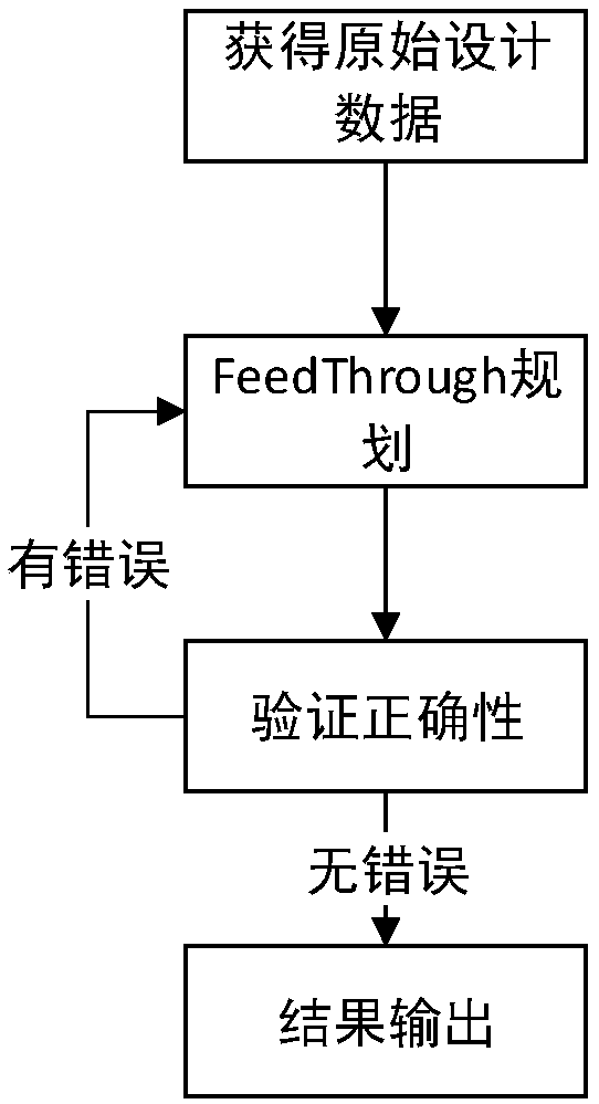
[0036] The invention discloses an automatic planning method for integrated circuit semi-customized physical design through signal lines. The specific implementation modes of the invention will be further described below in combination with preferred embodiments.

[0037] It is worth mentioning that those skilled in the art should note that the "FeedThrough" involved in the patent application of the present invention is defined as a "through signal line" (through line, the same below); the "DEF" (Design Through) involved in the patent application of the present invention ExchangeFormat), which is defined as "design exchange format"; "Dijkstra", which is involved in the patent application of the present invention, is defined as "Dijkstra algorithm"; "Block", which is involved in the patent application for the present invention, is defined as "submodule ".

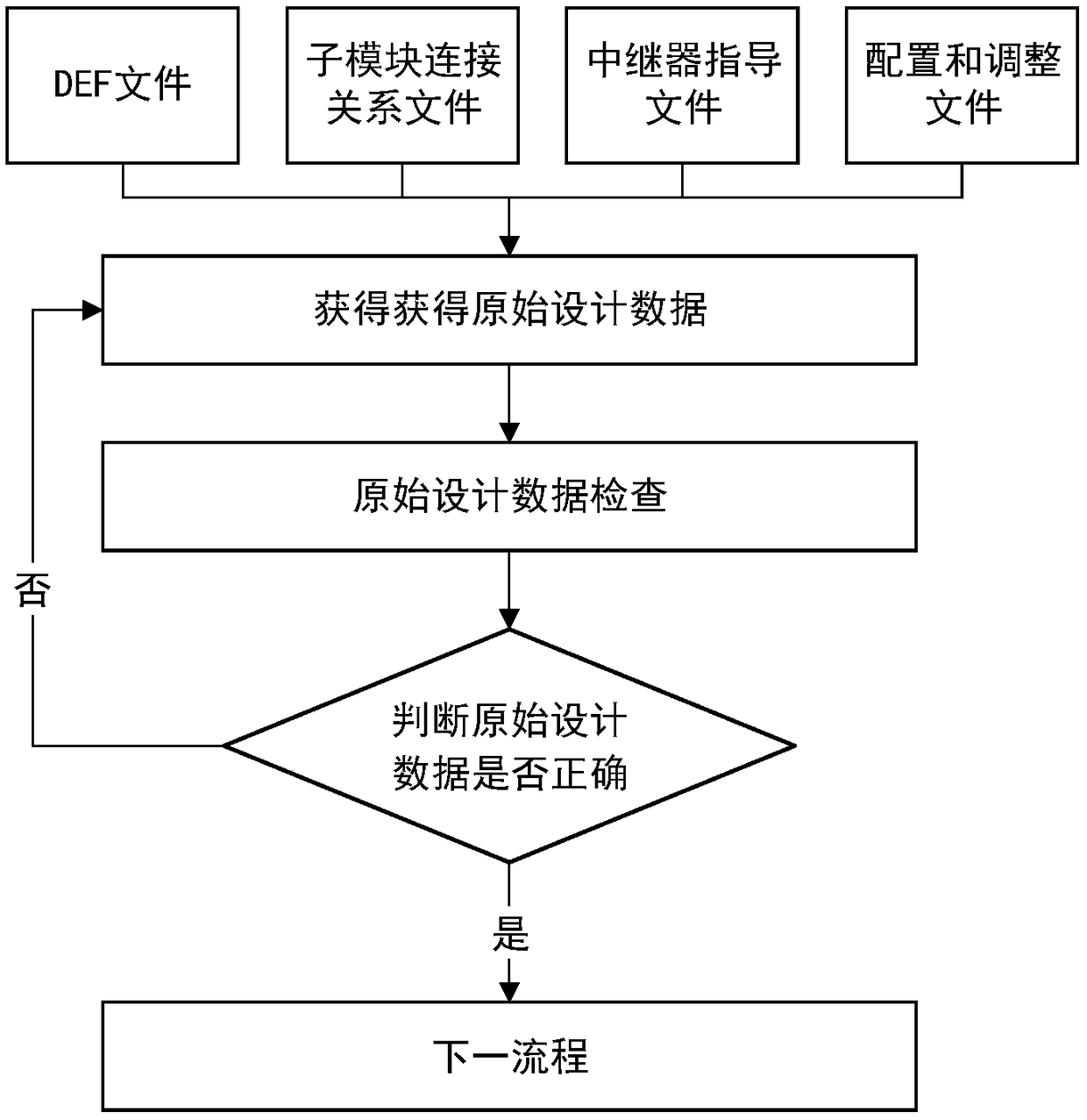
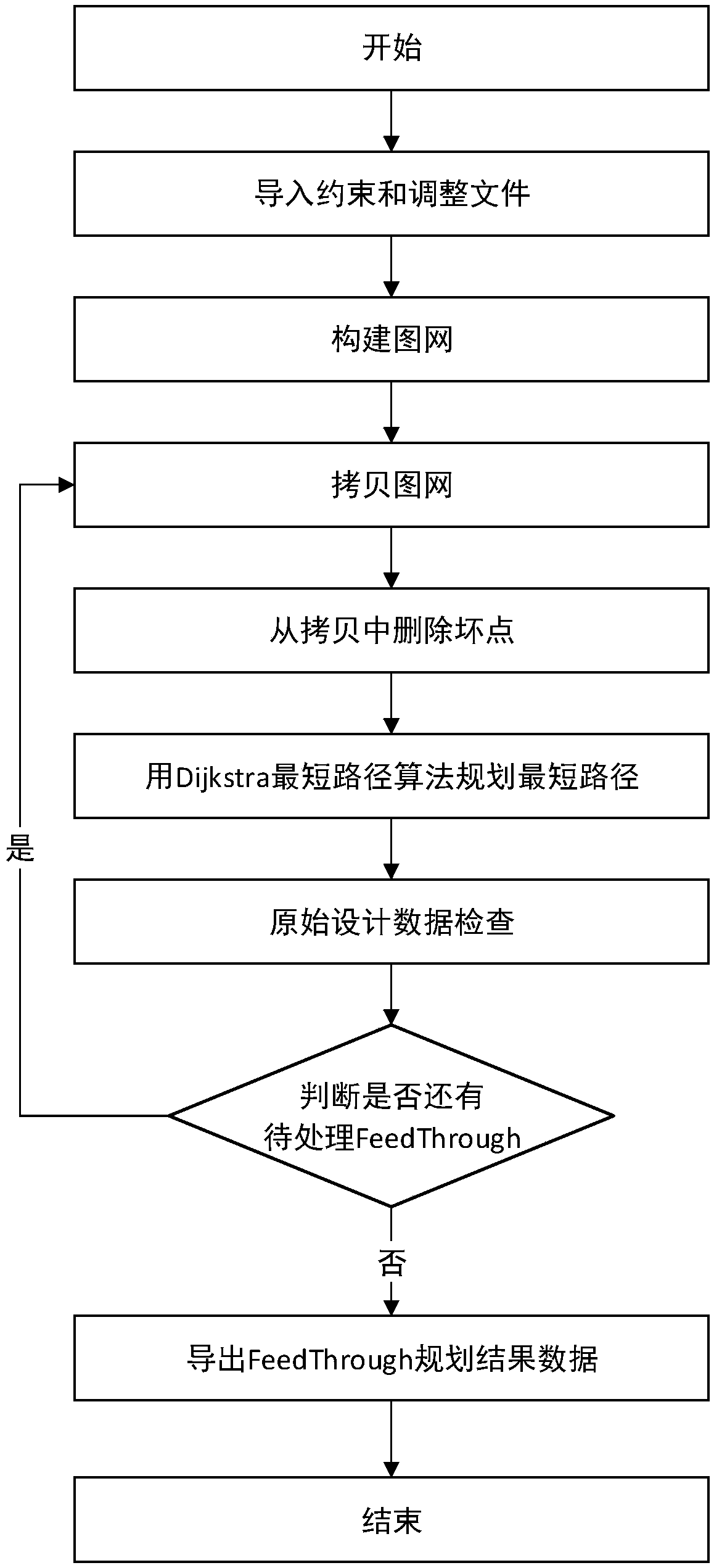
[0038] see attached figure 1 , figure 1 It shows the system flow of the automatic planning method for the integrated circ...


PUM


Abstract

The invention discloses an integrated circuit semi-custom physical design penetration signal line automatic planning method, comprising the following steps: Step S1: Obtain the original design data and judge the correctness of the original design data. If the judgment is passed, the step S1 is executed; otherwise, the step S1 is executed repeatedly. 2, carry out automatic planning of that pas signal line according to the original design data. 3, derive a through signal line planning result file accord with that format prescribed by the EDA tool and a report file for subsequent analysis, judging whether the through signal line plan result file conforms to the requirement, and executing a subsequent flow if the judgement is passed, otherwise repeatedly executing the step S1. The invention discloses an integrated circuit semi-custom physical design penetration signal line automatic planning method, which has the characteristics of short FeedThrough path, moderate number of sub-module pins, good FeedThrough symmetry and the like, and can improve the design efficiency of penetration signal line.

Description

technical field [0001] The invention belongs to the technical field of integrated circuit design automation, and in particular relates to an automatic planning method for integrated circuit semi-customized physical design through signal lines. Background technique [0002] As the scale of the chip becomes larger and larger, a top-down design method has to be used to divide the chip into different sub-modules, so that the original timing path is distributed in different sub-modules, causing each sub-module to be different from the Other submodules generate connection relationships. Since there will be millions of connection lines between different sub-modules in the chip, the FeedThrough (through signal line) planning of the chip is an important part of the entire back-end design process. [0003] At present, various design companies do not optimize the design during the FeedThrough planning process, which leads to problems such as poor design results and long design cycles,...

Claims


Application Information

Patent Timeline
Patent Type & Authority Applications(China)
IPC IPC(8): G06F17/50
CPCG06F30/392Y02E60/00
Inventor 徐靖
Owner 嘉兴倚韦电子科技有限公司
Why Eureka
Try Eureka