Method for manufacturing gallium nitride single crystal wafer

A gallium nitride monolithic and manufacturing method technology, which is applied in the field of manufacturing, can solve problems such as crystal defects, fractures, wafer deformation and warping, and achieve the effect of no crystal defects

Inactive Publication Date: 2019-03-01
WUXI WUYUE SEMICON CO LTD
View PDF7 Cites 5 Cited by
  • Summary
  • Abstract
  • Description
  • Claims
  • Application Information

AI Technical Summary

Problems solved by technology

Therefore, when GaN crystals are grown on substrates made of these materials, due to the difference in lattice constant and thermal expansion coefficient between the grown crystals and the substrate, stress will be generated inside the grown GaN, resulting in crystal defects or even fractures.
However, affected by the residual stress inside GaN, the whole wafer will be deformed and warped, which is also an inevitable problem.

Method used


Image

  • Method for manufacturing gallium nitride single crystal wafer
  • Method for manufacturing gallium nitride single crystal wafer
  • Method for manufacturing gallium nitride single crystal wafer

Examples


example 1

[0024] Example 1 (HVPE method combined with two-stage growth method to produce a single GaN wafer)

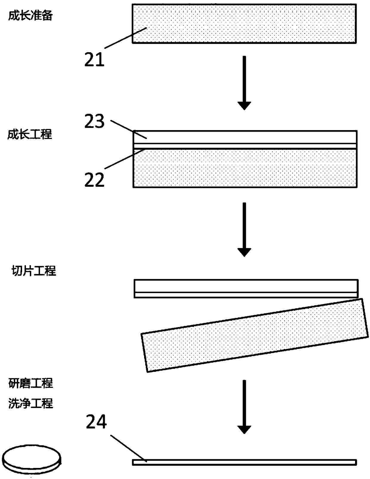
[0025] figure 2 The schematic diagram of the manufacturing process of Example 1 implemented based on the method of the present invention (manufacturing of a single GaN wafer) and its process flow (preparation stage for crystal growth—crystal growth process—crystal slicing process—grinding and cleaning process) are shown. After completing various preparations before crystal growth (detailed steps are painstakingly omitted here), the GaN buffer layer 22 and the GaN epitaxial layer 23 are grown on the SCAM substrate 21 by using the HVPE method combined with the two-stage growth method. The GaN layer is stripped from the SCAM substrate, and the stripped GaN layer is ground and cleaned to obtain a finished GaN single crystal substrate 24.

[0026] (1) Crystal growth process of GaN buffer layer

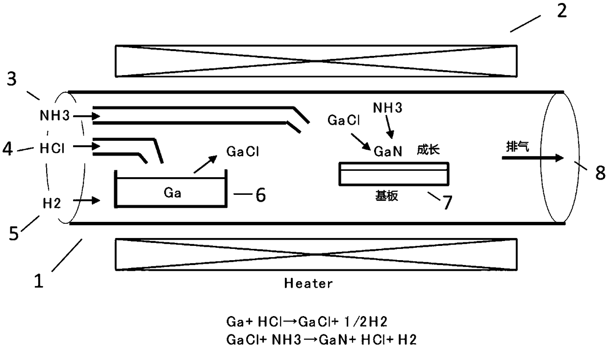
[0027] A 2 inch diameter SCAM substrate was placed on a pedestal (not shown in the fi...

example 2

[0034] Example 2 (HVPE method combined with two-stage growth method to produce GaN crystal ingot and multiple wafers)

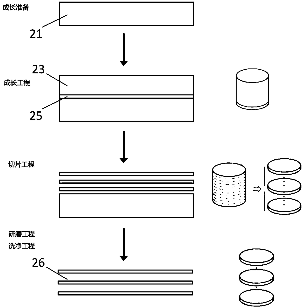
[0035] image 3 A schematic diagram of the manufacturing process implemented based on the method of the present invention (fabrication of GaN crystal ingots and multiple wafers) is shown. After completing a series of preparatory work in advance (the detailed steps are omitted here), the HVPE method combined with the two-stage growth method was used to complete the In growth process on the SCAM substrate 21. x Ga 1-x Fabrication of N (x=0.17) layer 25 and GaN epitaxial layer 23 . The GaN crystal ingot is peeled off from the SCAM substrate, and several GaN wafers 26 are obtained after a slicing process, a grinding process, and a cleaning process.

[0036] (1)In x Ga 1-x Crystal growth process of N(x=0.17) layer

[0037] A SCAM substrate 7 with a diameter of 2 inches was placed on a susceptor (not shown in the figure) in the reaction furnace 1 (HVPE appara...


PUM

PropertyMeasurementUnit
thicknessaaaaaaaaaa
thicknessaaaaaaaaaa
thicknessaaaaaaaaaa

Abstract

The invention belongs to the manufacturing method, and particularly relates to a method for manufacturing a gallium nitride single crystal wafer. The method for manufacturing the gallium nitride single crystal wafer comprises the following steps of carrying out crystallizing of gallium nitride by using an HVPE two-stage growth method on an (ScAlMgO4) substrate. The method has the remarkable effects that the maximum characteristic of the GaN crystallizing is embodied in the crystal quality and the size of the wafer. In the invention, the lattice constant and the thermal expansion coefficient ofthe GaN substrate are basically consistent with those of an SCAM substrate, so that the manufacturing of the high-quality GaN crystal without dislocation and crystallization defects can be realized.

Description

technical field [0001] The invention belongs to a manufacturing method, in particular to a manufacturing method of a gallium nitride single crystal wafer. Background technique [0002] Semiconductor components such as semiconductor laser diodes, light-emitting diodes, and transistors are manufactured in high-quality thin-film crystal layers laminated on the substrate according to the integration conditions of the crystal lattice. In other words, the lattice integration technology between the thin film crystal layer and the substrate determines whether it is possible to realize the manufacture of high-quality crystals with few crystal defects. The manufacture of GaN blue light LED, which shined in the Nobel Prize in 2014, was manufactured on a sapphire substrate because there was no high-quality GaN substrate at that time. Since the crystal lattice between the sapphire substrate and the GaN layer is not integrated, the density of crystalline defects called threading dislocat...

Claims


Application Information

Patent Timeline
Patent Type & Authority Applications(China)
IPC IPC(8): H01L21/02H01L21/20H01L21/205
CPCH01L21/0242H01L21/02458H01L21/0254H01L21/0262H01L21/02634H01L21/2011H01L21/2056
Inventor 张海涛
Owner WUXI WUYUE SEMICON CO LTD
Why Eureka
Try Eureka