Lighting device and lighting device

A light-emitting device and optical path technology, which is applied to lighting devices, lighting device components, signal devices, etc., can solve the problems of a larger deflection angle, an increased range, and an increased rate of change of the optical path length of a light deflecting portion. achieve the effect of miniaturization

Active Publication Date: 2020-07-31
PANASONIC INTELLECTUAL PROPERTY MANAGEMENT CO LTD
View PDF7 Cites 0 Cited by
  • Summary
  • Abstract
  • Description
  • Claims
  • Application Information

AI Technical Summary

Problems solved by technology

Therefore, in the case where the phosphor is formed on a flat surface and the scanning area of ​​the excitation light is set to a certain size, the rate of change of the optical path length increases as the scanning area of ​​the excitation light approaches, so that it cannot sufficiently The excitation light is concentrated, and the diameter of the bright spot on the phosphor is enlarged
Furthermore, in the case of an optical system configuration in which the incident angle of the phosphor is large, there is a problem that the bright spot is greatly inclined as the scanning position of the excitation light approaches both ends.
In addition, in order to scan a certain distance, it is necessary to increase the deflection angle of the light deflection unit. According to the method of driving the movable mirror with a magnetic circuit, the heat resistance of the coil due to the increase in current and the strength of the spring holding the mirror Durability can be an issue
In addition, the increase of the deflection angle of the light deflection unit leads to an increase in the range (effective range) in which the excitation light irradiates the optical element on the scanning optical path, which leads to problems such as an increase in the size of the device and an increase in the cost of the optical components.
[0013] On the other hand, as in Patent Document 2, when the condensing optical system is arranged between the light deflection unit and the phosphor, the light beam is refracted toward the focus direction of the condensing optical system due to the refraction effect of the lens on the deflected light beam. Therefore, Sensitivity (i.e., amount of displacement) on the phosphor to deflection angle is reduced
Therefore, it is necessary to design the deflection angle by the light deflection part to be large, which also causes the above-mentioned problems in this case.

Method used


Image

  • Lighting device and lighting device
  • Lighting device and lighting device
  • Lighting device and lighting device

Examples


Embodiment 1

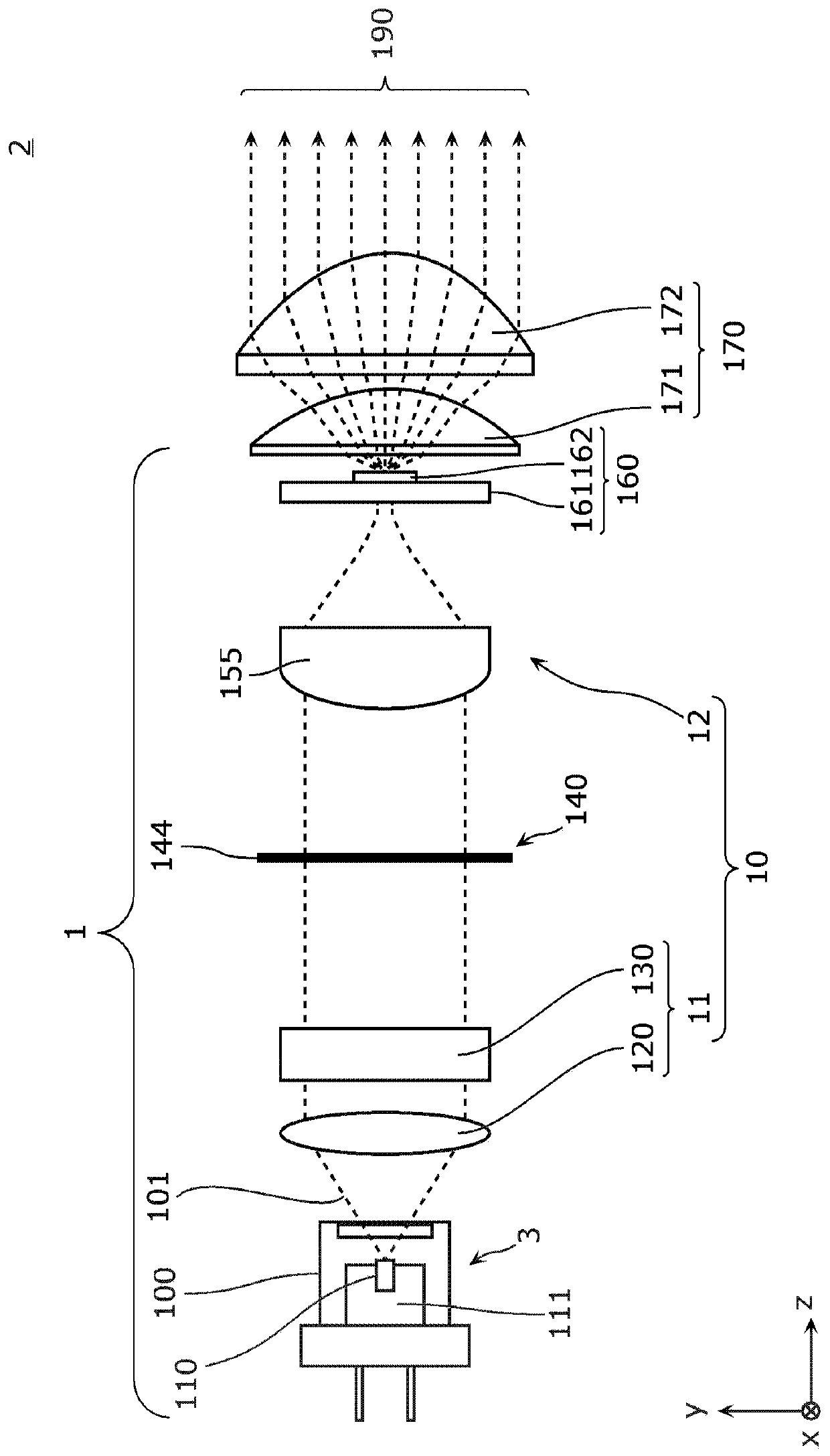
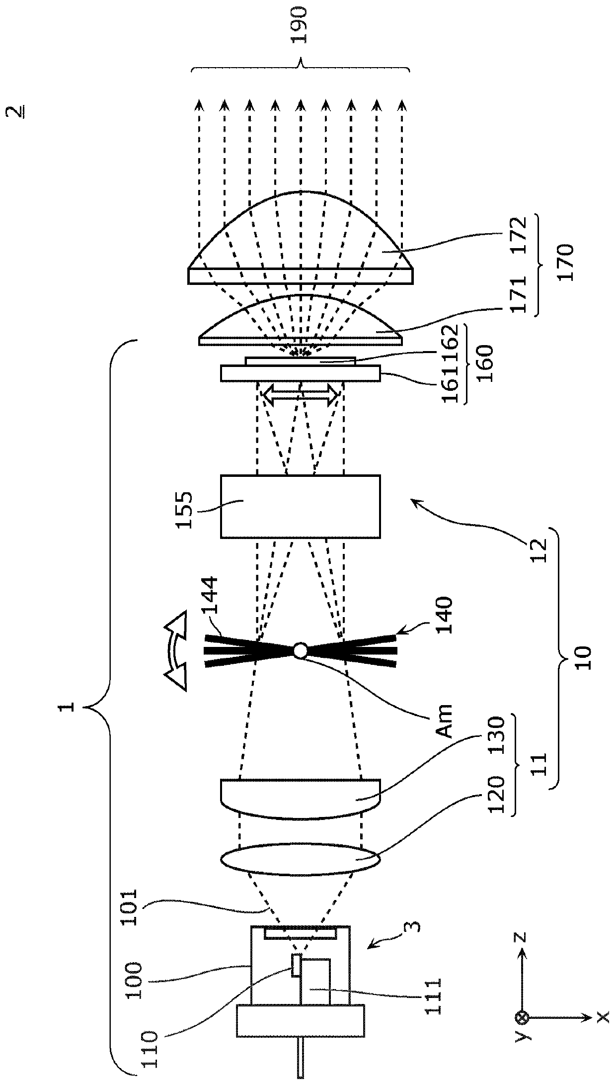
[0048] figure 1 as well as figure 2 It is a side view and a plan view showing the configuration of the simplest optical system of the light emitting device 1 and the lighting device 2 according to the present embodiment, respectively. exist figure 1 as well as figure 2 Here, the optical axis direction of the projection light 190 projected from the illumination device 2 is defined as the z-axis direction, and two directions perpendicular to the optical axis direction and orthogonal to each other are defined as the x-axis direction and the y-axis direction.

[0049] The lighting device 2 related to this embodiment is a device that emits projection light 190, such as figure 1 as well as figure 2 It is shown that the light emitting device 1 and the projection optical system 170 are provided. The light emitting device 1 includes a light source unit 3 , a light deflection unit 140 , a wavelength conversion unit 160 , and a light collection unit 10 .

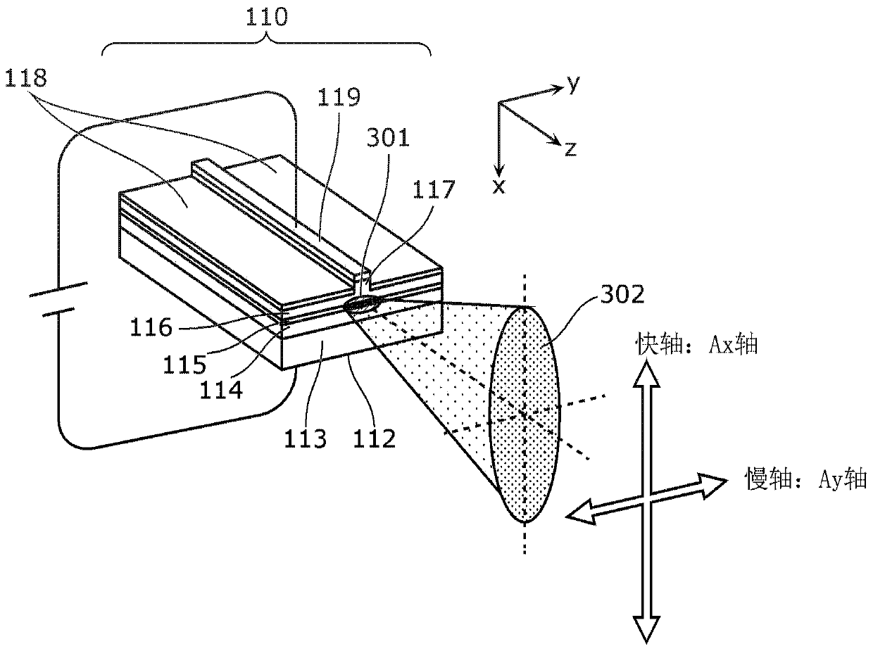
[0050] The light sourc...

Embodiment 2

[0110] A light-emitting device and an illuminating device according to Example 2 will be described. In this embodiment, the difference from Embodiment 1 is that two semiconductor laser light sources are used. Hereinafter, the present embodiment will be described with reference to the drawings focusing on points of difference from the first embodiment.

[0111] Figure 7 as well as Figure 8 These are a side view and a perspective view showing the optical system configurations of the light emitting device 1a and the lighting device 2a according to the present embodiment, respectively.

[0112] Such as Figure 7 as well as Figure 8 As shown, the lighting device 2 a according to this embodiment includes the light emitting device 1 a and the projection optical system 170 .

[0113] Such as Figure 7 As shown, the light emitting device 1 a includes a light source unit 3 a, a light collecting unit 10 a, a light deflecting unit 140 a, and a wavelength converting unit 160 a. T...


PUM


Abstract

Equipped with: a light source unit (3), which emits excitation light (101); a light deflection unit (140), which deflects the excitation light (101); a wavelength conversion unit (160), which is irradiated with the excitation light deflected by the light deflection unit (140) (101), convert the excitation light (101) into wavelength converted light with different wavelengths to emit; ), the first optical system (11) arranged between the light source part (3) and the light deflection part (140), and the first optical system (11) arranged between the light deflection part (140) and the wavelength conversion part (160) Two optical systems (12) constitute, in the section perpendicular to the direction of travel of the excitation light (101), the axis of the direction in which the beam parameter product of the excitation light (101) becomes the minimum is set as the Ax axis, and the axis perpendicular to the Ax axis is When the axis of the direction is the Ay axis, in the second optical system (12), the focus distance in the Ay axis direction is smaller than the focus distance in the Ax axis direction.

Description

technical field [0001] The present disclosure relates to a light emitting device that irradiates a wavelength conversion unit with excitation light emitted from a light source unit to cause the wavelength conversion unit to generate light different from the excitation light, and an illumination device including the light emitting device. Background technique [0002] Illumination devices using laser light sources such as semiconductor light emitting elements (semiconductor laser elements) include spot lighting, vehicle headlights, projectors, endoscope lighting, and the like. In these illuminating devices, a wavelength converter composed of a phosphor represented by yttrium aluminum garnet (YAG) is irradiated with laser light having a wavelength near 400 nm or near 450 nm, and the fluorescence generated by the excitation of the phosphor, Alternatively, emitted light composed of fluorescence and scattered components of excitation light is used as illumination light. In such ...

Claims


Application Information

Patent Timeline
Patent Type & Authority Patents(China)
IPC IPC(8): F21K9/20F21K9/64F21K9/65F21V14/06F21V14/04H01S5/022F21V13/04G02B13/18G02B13/00G02B17/08F21V7/04G02B19/00F21V5/04F21V5/02G02B5/20F21Y115/30
CPCF21S2/00F21V5/04F21V7/04F21V13/00F21V14/04F21V14/06G02B13/00G02B13/18G02B17/08G02B19/00G02B5/20F21S41/635F21S41/285F21S41/255F21S41/321F21S41/365F21S41/176F21S41/675F21S41/16F21S41/173F21S41/37G02B26/0833H01S5/0609
Inventor 村上公博
Owner PANASONIC INTELLECTUAL PROPERTY MANAGEMENT CO LTD
Why Eureka
Try Eureka