

Solid imaging device, method for manufacturing the same, and camera using the same
A technology for a solid-state imaging device and a manufacturing method, which is applied to radiation control devices, image communications, televisions, etc., can solve the problems of inability to stably form a transmission layer, inability to fully guarantee the optical path length, and the reduction of pixel light-concentration efficiency, etc. The effect of optimization, reduction of manufacturing variation, and high condensing efficiency
- Summary
- Abstract
- Description
- Claims
- Application Information
AI Technical Summary
Problems solved by technology
Method used
Image

Examples
no. 1 Embodiment approach
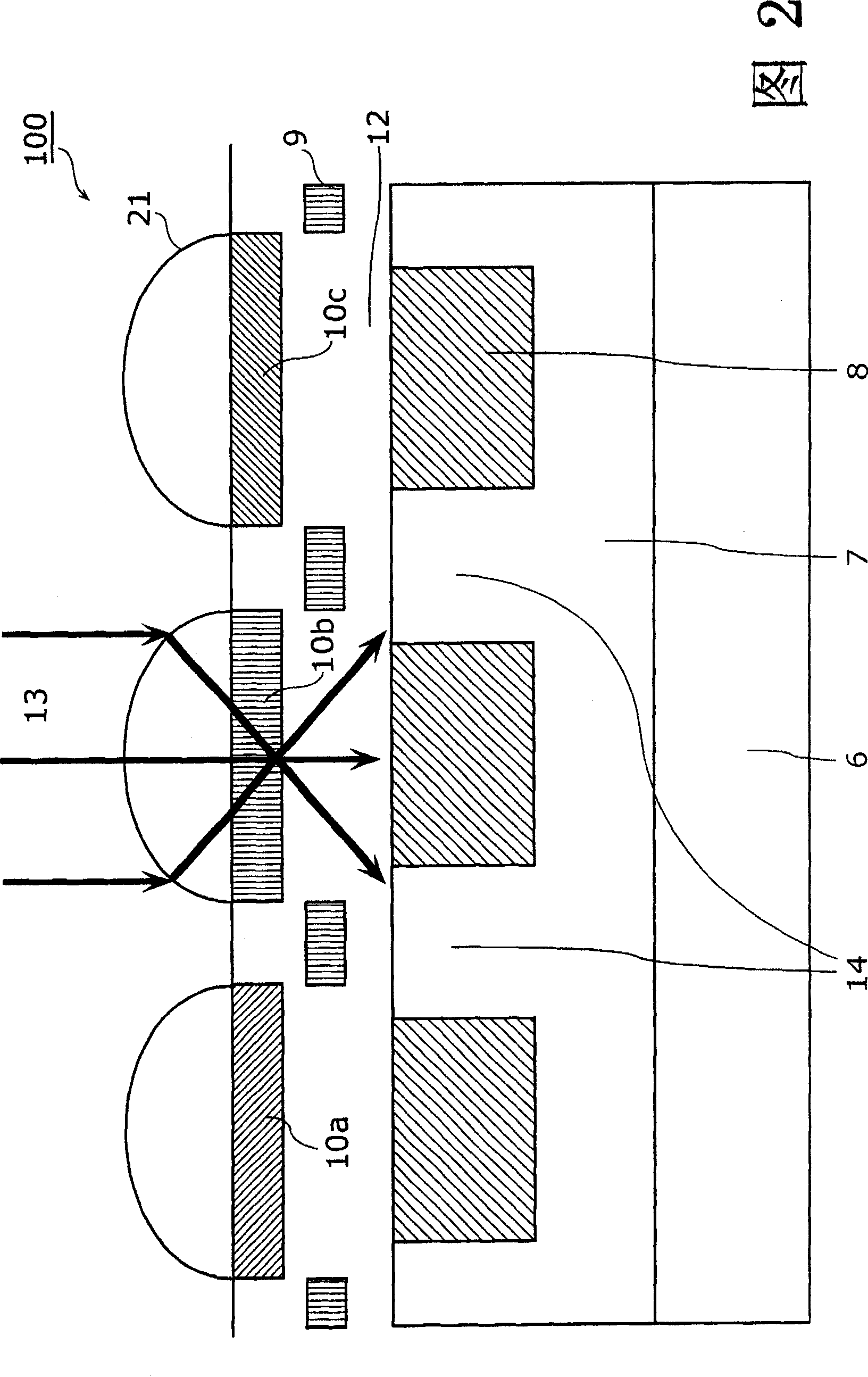
[0087] 3 is a cross-sectional view of a pixel portion of the solid-state imaging device according to the first embodiment of the present invention. In the solid-state imaging device 101 (only three pixels are shown) shown in FIG. 3 , a P-type layer 7 is formed on the N-type layer 6 , and a photodiode 8 is formed in the P-type layer 7 . A light shielding film 9 for shielding light is formed above the isolation region 14 for isolating the photodiodes 8 . In addition, an interlayer insulating film 12, color filters 10a to 10c that transmit only the color light corresponding to each pixel, and the vertically-shaped light of the present invention for condensing incident light 13 are formed on the photodiode 8. The transmissive layer 15 and the lens layer 11 having a concavo-convex shape formed on the upper portion and the periphery of the transmissive layer 15 . In addition, the shape of the transmissive layer 15 may be a cuboid, a cylinder, or the like. In addition, the material...
no. 2 Embodiment approach
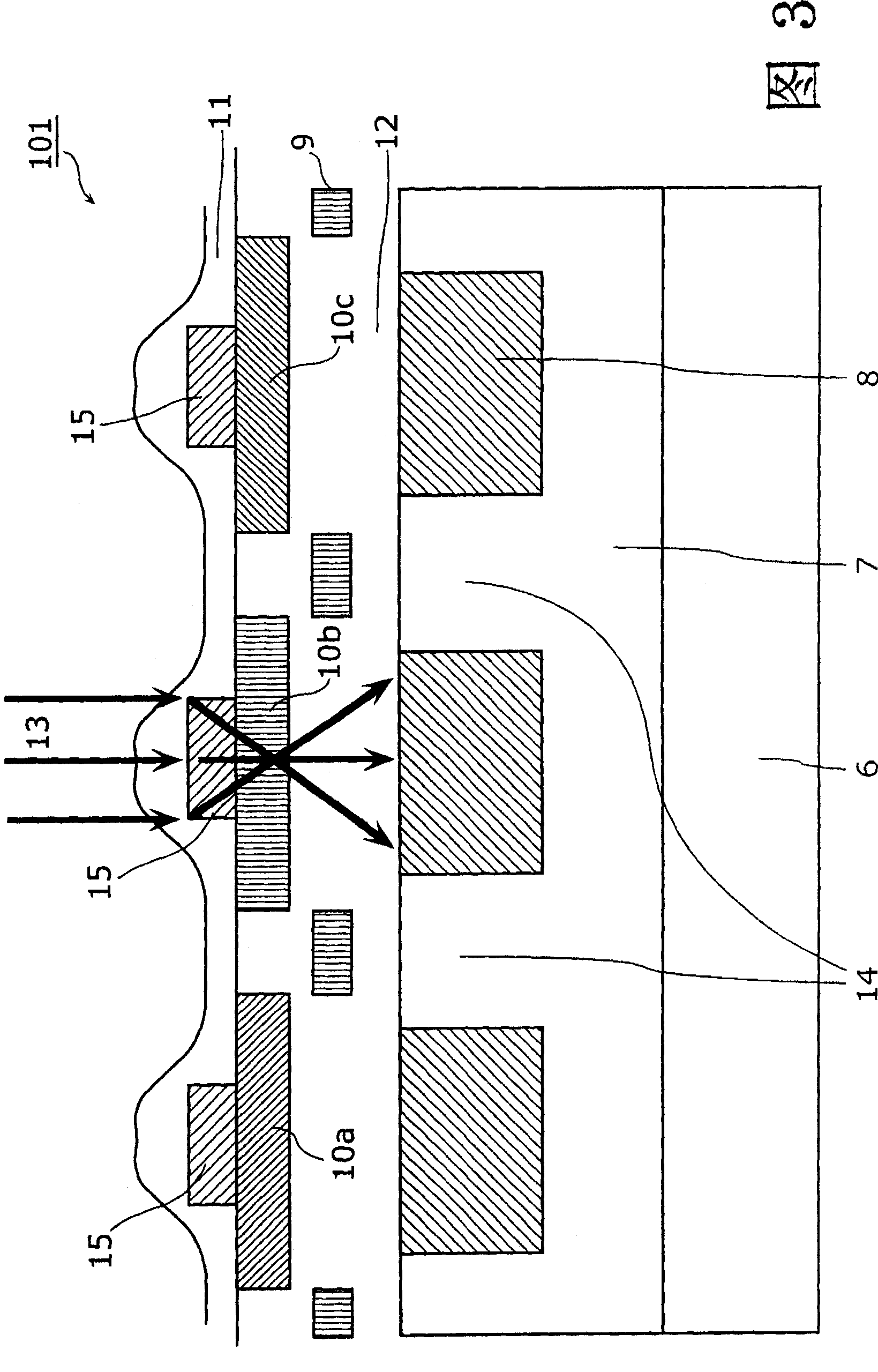
[0090] 4 is a cross-sectional view of a pixel portion of a solid-state imaging device according to a second embodiment of the present invention. Here, the difference from the first embodiment is that in the solid-state imaging device 102, the width and height of the vertically shaped transmissive layer of the present invention are determined according to various colors of red (R), green (G) and blue (B). The unit pixels corresponding to the colors are optimally changed, correspondingly, the concavo-convex shape of the lens layer 11 is changed, and the focal lengths relative to the light of each color are respectively set to optimal focal lengths. In particular, since the refractive index of the transmissive layer 15 increases on the short wavelength side and conversely decreases on the long wavelength side, it is necessary to adjust the size of the transmissive layer.
[0091] Among the transmissive layers 15a, 15b, and 15c, the transmissive layer 15a has the smallest width an...
no. 3 Embodiment approach
[0093] 5( a ) to ( e ) are explanatory views of a method of manufacturing the light-condensing element of the solid-state imaging device according to the third embodiment of the present invention.
[0094] First, as shown in FIG. 5( a ), on the upper portion of the base 201 (the color filters 10 a to 10 c in the first and second embodiments described above), a film containing SiO? The transmissive layer material 202. Next, as shown in FIG. 5( b ), a resist film 203 is formed on the upper portion of the transmissive layer material 202 , and as shown in FIG. 5( c ), the resist film 203 other than a predetermined portion is removed by photolithography. And further, as shown in FIG. 5( d ), dry etching technique is used to remove the transmissive layer material 202 outside the specified area. Then as shown in Fig. 5(e), using a higher viscosity than SiO? The material (BPSG film, TEOS film, benzocyclobutene, polyimide resin, etc.) is used to form the lens layer 204 on the entire ...
PUM
 Abstract
Description
Claims
Application Information