Method for manufacturing printed circuit board

A technology for printed circuit boards and manufacturing methods, applied in the fields of printed circuit manufacturing, printed circuit, multilayer circuit manufacturing, etc., can solve the problems of thin signal layer and easy diffusion of ink droplets, etc., achieve high material utilization rate and ensure the effect of precision

Inactive Publication Date: 2019-03-08
SHENZHEN JINZHOU PRECISION TECH
View PDF4 Cites 9 Cited by
  • Summary
  • Abstract
  • Description
  • Claims
  • Application Information

AI Technical Summary

Problems solved by technology

[0004] The purpose of the present invention is to provide a method for manufacturing a printed circuit board to solve the technical problems in the prior art that the signal layer is relatively thin during single-layer printing and the ink droplets are easy to spread during multi-layer printing in the high-precision inkjet printing technology.

Method used


Image

  • Method for manufacturing printed circuit board
  • Method for manufacturing printed circuit board
  • Method for manufacturing printed circuit board

Examples


specific Embodiment approach

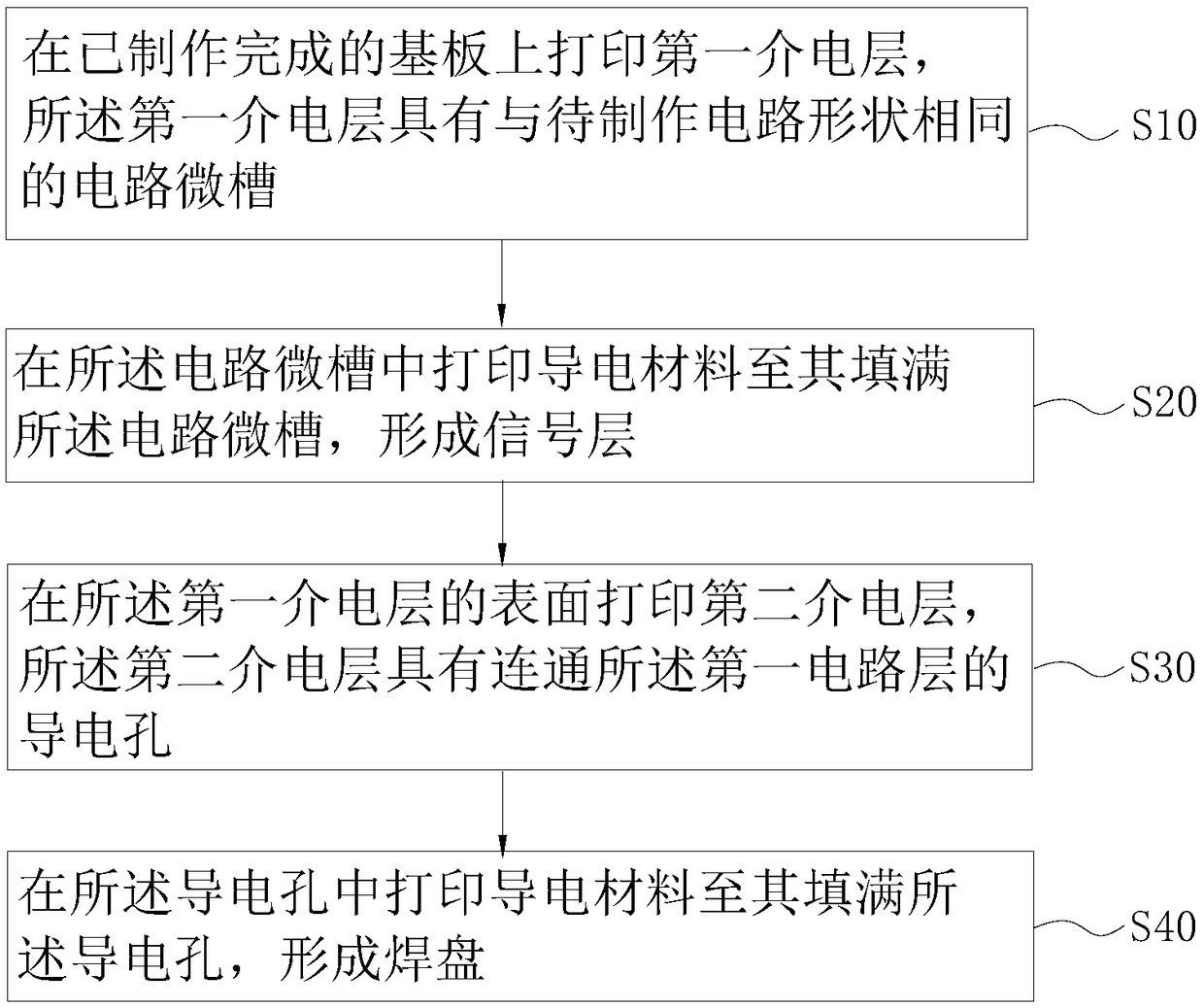
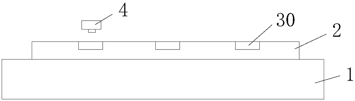
[0049] Further, as a specific implementation of the method for manufacturing a printed circuit board provided by the present invention, step S10 includes:

[0050] placing or printing an insulating layer completely covering the substrate 1 on the completed substrate 1;

[0051] According to the shape of the circuit to be fabricated, the circuit microgroove 30 is etched out by laser etching to form the first dielectric layer 2 .

[0052] In this embodiment, there is no hole or groove on the insulating layer, and the area corresponding to the circuit to be fabricated and the area corresponding to the first dielectric layer 2 are completely covered, and the material of the insulating layer is completely consistent with the material of the first dielectric layer 2. Similarly, after printing, laser etching is used to etch circuit microgrooves. The insulating layer can also be printed by inkjet printing equipment. Before printing, the shape and position information of the insulatin...


PUM


Abstract

The invention provides a method for manufacturing a printed circuit board. The method comprises the following steps: printing a first dielectric layer on a fabricated substrate, wherein the first dielectric layer has a circuit micro slot in the same shape as the circuit to be fabricated; printing conducting material in the circuit micro slot until the circuit micro slot is filled to form a signallayer; printing a second dielectric layer on the surface of the first dielectric layer, wherein the second dielectric layer has a conducting hole communicated with the signal layer; and printing conducting material in the conducting hole until the conducting hole is filled to form a pad. The method for manufacturing a printed circuit board provided by the invention prints the first dielectric layer having the circuit micro slot on the substrate, and prints the conducting material in the circuit micro slot. The dielectric layers and signal layer are respectively manufactured by printing, with no need to manufacture a circuit board by adopting traditional processes such as exposure, development, etching and electroplating, which causes no environmental pollution.

Description

technical field [0001] The invention belongs to the technical field of manufacturing printed circuit boards, and more specifically relates to a method for manufacturing printed circuit boards. Background technique [0002] In a large number of electronic products such as mobile phones and computers, there are Printed Circuit Boards (PCB for short), which integrate circuits into the circuit board to facilitate wiring. The printed circuit board is mainly composed of a dielectric layer and a signal layer. The circuit of the signal layer is a micro circuit. The characteristic line width of the circuit is between 80 μm and 150 μm, and the thin line can even reach 50 μm. The characteristic line width is 18 μm / 35 μm / 70 μm . At present, printed circuit boards are usually manufactured by relatively mature processes such as exposure, development, etching, and electroplating. However, processes such as developing, etching, and electroplating use a large amount of chemical reagents, an...

Claims


Application Information

Patent Timeline
Patent Type & Authority Applications(China)
IPC IPC(8): H05K3/10H05K3/40H05K3/46H05K3/00H05K1/09
Inventor 屈建国
Owner SHENZHEN JINZHOU PRECISION TECH
Why Eureka
Try Eureka