Filter packaging structure and packaging method

A packaging structure and packaging method technology, which is applied in the manufacture of semiconductor devices, electrical solid state devices, semiconductor/solid state devices, etc., can solve problems such as poor filter size consistency, obstacles to miniaturization of RF front-end systems, and influence of filter parameters.

Active Publication Date: 2020-10-20
SHANGHAI INST OF MICROSYSTEM & INFORMATION TECH CHINESE ACAD OF SCI
View PDF4 Cites 0 Cited by
  • Summary
  • Abstract
  • Description
  • Claims
  • Application Information

AI Technical Summary

Problems solved by technology

Traditional filters are generally made on PCB substrates or ceramic substrates, but the dielectric constant, thickness of the substrate material, and the size consistency of the filter are poor, especially in relatively high frequency bands, these errors will affect the parameters of the filter have a greater impact
At the same time, the completed discrete components need to be surface-mounted on the PCB board together with other active and passive chips. This method often takes up a large area, which creates a huge obstacle to the miniaturization of the RF front-end system.

Method used


Image

  • Filter packaging structure and packaging method
  • Filter packaging structure and packaging method
  • Filter packaging structure and packaging method

Examples


Embodiment 1

[0090] see figure 1 , the present invention provides a packaging method for a filter packaging structure, the packaging method for the filter packaging structure includes the following steps:

[0091] 1) providing a high-resistance silicon substrate, the high-resistance silicon substrate includes opposite first surfaces and second surfaces;

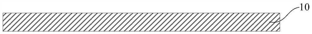
[0092] 2) Forming a groove with a predetermined depth on the first surface of the high-resistance silicon substrate, and forming a through-silicon via in the high-resistance silicon substrate, and forming a through-silicon via along the high-resistance silicon substrate. The thickness direction runs through the high-resistance silicon substrate;

[0093] 3) forming an insulating layer on the inner wall of the TSV;

[0094] 4) Filling the TSV with a metal layer to form a conductive TSV structure, the conductive TSV structure includes a signal line and a connection ground line, the connection ground line surrounds the signal line, and ha...

Embodiment 2

[0142] Please combine Figure 2 to Figure 19 read on Figure 20, the present invention also provides a filter packaging structure, the filter packaging structure includes: a high-resistance silicon substrate 10, the high-resistance silicon substrate 10 includes a first surface and a second surface opposite; the high-resistance silicon substrate A groove 12 is formed on the first surface of 10, and a through-silicon hole 14 is formed in the high-resistance silicon substrate 10, and the through-silicon hole 14 penetrates the high-resistance silicon substrate 10 along the thickness direction of the high-resistance silicon substrate 10. Silicon substrate 10; a conductive TSV structure 16, the conductive TSV structure 16 is located in the TSV 14; the conductive TSV structure 16 includes a signal line 162 and a connection ground line 161, The connection ground line 161 surrounds the signal line 162 and has a distance from the signal line 162; the first ground line 191, the first gr...


PUM

PropertyMeasurementUnit
electrical resistivityaaaaaaaaaa
thicknessaaaaaaaaaa

Abstract

The invention provides a filter packaging structure and a packaging method thereof. The method comprises the following steps of 1) providing a high-resistance silicon substrate; 2) forming a groove with a preset depth in a first surface of the high-resistance silicon substrate, and forming a through silicon via in the high-resistance silicon substrate; 3) forming an insulating layer on the inner wall of the through silicon via; 4) forming a conductive through silicon via structure; 5) forming a first ground wire and a second ground wire, and forming a first dielectric layer; 6) forming a second dielectric layer, and forming a third dielectric layer; 7) forming a first transmission line, and forming a second transmission line; and 8) forming a fourth dielectric layer, and forming a third transmission line. The high-resistance silicon substrate is adopted as a chip substrate of a filter; the filter is connected with the substrate through a micro-strip line transmission structure; and theconductive through silicon via structure on the high-resistance silicon substrate leads a lead to the back surface of the high-resistance silicon substrate, so that the lead can be directly connectedwith a packaging substrate in a vertical direction and can be interconnected with other devices in a packaging body.

Description

technical field [0001] The invention belongs to the technical field of semiconductors, and in particular relates to a filter packaging structure and a packaging method thereof. Background technique [0002] The rapid development of the wireless communication industry puts forward higher requirements for microwave filters: better performance, smaller size, lighter weight and lower cost. Traditional filters are generally made on PCB substrates or ceramic substrates, but the dielectric constant, thickness of the substrate material, and the size consistency of the filter are poor, especially in relatively high frequency bands, these errors will affect the parameters of the filter cause a relatively large impact. At the same time, the completed discrete components need to be surface-mounted on the PCB together with other active and passive chips. This method often takes up a large area, which creates a huge obstacle to the miniaturization of the RF front-end system. Contents o...

Claims


Application Information

Patent Timeline
Patent Type & Authority Patents(China)
IPC IPC(8): H01L21/50H01L21/60H01L23/48H01L23/528H01L23/367
CPCH01L21/50H01L23/367H01L23/48H01L23/528H01L24/85H01L2224/85
Inventor 张伟博罗乐徐高卫
Owner SHANGHAI INST OF MICROSYSTEM & INFORMATION TECH CHINESE ACAD OF SCI
Why Eureka
Try Eureka