A kind of crystal-bonding structure and crystal-bonding method of flip-chip LED light-emitting chip

A light-emitting chip and solid crystal technology, which is applied in the direction of electric solid-state devices, semiconductor/solid-state device manufacturing, semiconductor/solid-state device components, etc., can solve the problem of short circuit between two electrodes, avoid short circuit, reduce process difficulty, and avoid virtual soldering Effect

Active Publication Date: 2020-09-18
CHANGCHUN CEDAR ELECTRONICS TECH CO LTD
View PDF2 Cites 0 Cited by
  • Summary
  • Abstract
  • Description
  • Claims
  • Application Information

AI Technical Summary

Problems solved by technology

If you want to ensure that the two electrodes of the LED light-emitting chip are in full contact with the pads, the distance between the two pads needs to be small enough to ensure that the electrodes and the pads are in full contact. However, due to the PCB processing technology, it is difficult to achieve a pad spacing of less than 4mil. Assuming it can be made very small, due to the short distance between the pads and the fluidity of the solder, it is easy to cause a short circuit between the two electrodes

Method used

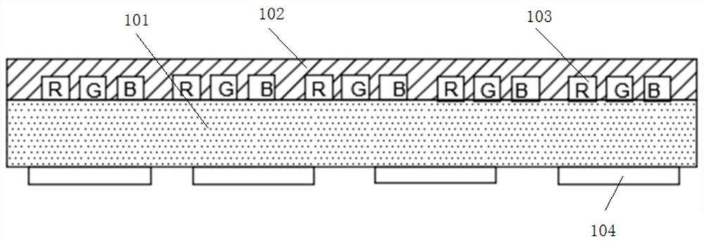

Image

  • A kind of crystal-bonding structure and crystal-bonding method of flip-chip LED light-emitting chip
  • A kind of crystal-bonding structure and crystal-bonding method of flip-chip LED light-emitting chip
  • A kind of crystal-bonding structure and crystal-bonding method of flip-chip LED light-emitting chip

Examples


Embodiment 1

[0033] Such as Figure 7 As shown, the red LED light-emitting chip 501 adopts a vertical die-bonding structure, which requires wire bonding, while the green LED light-emitting chip 502 and blue LED light-emitting chip 503 adopt a flip-chip die-bonding structure, which does not require wire bonding, effectively saving pads Design area, reduce wire bonding area, improve contrast.

Embodiment 2

[0035] Such as Figure 8 As shown, the red LED light-emitting chip 501 and the blue LED light-emitting chip 503 adopt a vertical die-bonding structure, which requires wire bonding; the green LED light-emitting chip 502 adopts a flip-chip die-bonding structure, which does not require wire bonding, effectively saving pads Design area, reduce wire bonding area, improve contrast.

Embodiment 3

[0037] Such as Figure 9 As shown, the red LED light-emitting chip 501 and the green LED light-emitting chip 502 adopt a vertical die-bonding structure, which requires wire bonding; the blue LED light-emitting chip 503 adopts a flip-chip die-bonding structure, which does not require wire bonding, effectively saving pads Design area, reduce wire bonding area, improve contrast.


PUM


Abstract

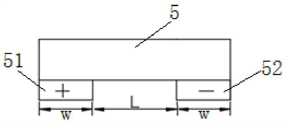
The present invention relates to a flip-chip LED light-emitting chip solid crystal structure and a solid crystal method thereof. A positive electrode and a negative electrode of the flip-chip LED light emitting chip of the solid crystal structure are respectively soldered to a positive electrode pad and a negative electrode pad through positive electrode solders and negative electrode solders; positive electrode solders and negative electrode solders are respectively printed on edges opposite to the positive electrode pad and the negative electrode pad; the positive electrode solders and the negative electrode solders are partially printed on the positive electrode pad and the negative electrode pad 12 respectively, and partially printed on a PCB board; a solder mask is printed on the PCBand locates between the positive electrode solder and the negative electrode solders; the solder mask is made of insulating materials; the solders are printed onto the positive electrode pad and the negative electrode pad of the PCB board through openings in a steel mesh using a printer. The structure reduces process difficulty, can ensure contact area between the two electrodes of the flip-chip LED light-emitting chip and the solders, and can avoid short circuit caused by flowing of the solders while avoiding the false soldering.

Description

technical field [0001] The invention belongs to the technical field of LED display screens, and relates to a crystal-bonding structure of a flip-chip LED light-emitting chip and a crystal-bonding method thereof. Background technique [0002] At present, LED chip technology is developing rapidly, and the development of flip-chip is particularly rapid. The natural advantage of flip-chip is that the light-emitting surface is large and the brightness is high. On the other hand, the electrode of flip-chip is under the chip. This design is more suitable for the production of COB small-pitch LEDs. display screen. [0003] In the field of small-pitch LEDs, the current domestic mainstream products are mainly based on surface mount technology. There are two technical advantages of surface mount products: first, it is easy to realize the "mixing" of the finished product end with the surface mount device of the product, and realize the uniform effect of the whole screen; second, the us...

Claims


Application Information

Patent Timeline
Patent Type & Authority Patents(China)
IPC IPC(8): H01L23/488H01L25/075H01L21/50
CPCH01L21/50H01L23/488H01L25/0753H01L2224/48091H01L2924/19105H01L2924/00014
Inventor 王瑞光段健楠马新峰郑喜凤
Owner CHANGCHUN CEDAR ELECTRONICS TECH CO LTD
Why Eureka
Try Eureka