Check patentability & draft patents in minutes with Patsnap Eureka AI!

Micro LED array display device

A technology of LED arrays and display devices, applied in lighting devices, electrical components, circuits, etc., can solve the problems of increased size, complicated process and inconvenience, and achieve the effect of eliminating complexity and inconvenience

Active Publication Date: 2019-03-15
LUMENS
View PDF12 Cites 6 Cited by
  • Summary
  • Abstract
  • Description
  • Claims
  • Application Information

AI Technical Summary

Problems solved by technology

In this case, the size of the micro LED array display is increased since the elements responsible for signal control of the micro LED pixels should be formed separately in the peripheral area, and the data lines arrayed along the vertical and horizontal axes should be connected to the micro LEDs by wire bonding. pixels are connected, thus making the process complex and inconvenient
[0004] Moreover, when forming a plurality of micro-LED pixels on one substrate, due to technical limitations when forming structures for emitting red light, green light, and blue light on one substrate, it is used in micro-LED array display devices. In the case of LED light sources, in the past, there was a difficulty that it could only be reflected in a single color

Method used


Image

  • Micro LED array display device
  • Micro LED array display device
  • Micro LED array display device

Examples


Embodiment Construction

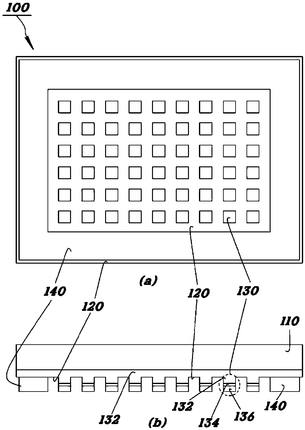
[0029] The present invention relates to a micro-LED array display device, which arrays micro-LED pixels through a mesa etching process (MESA etching) and flip-chip-welds the micro-LED pixels on a CMOS backplane, so that it can be applied to head-mounted displays ( Micro Display (Micro Display) such as Head Mounted Display (HMD) or Head Up Display (Head Up Display, HUD). In the present invention, micro-LED pixels are arranged through a mesa etching process when manufacturing LED chips, and are flip-chip welded on a CMOS backplane so that they can be driven individually. In addition, in the present invention, three elements of red, green and blue, that is, micro LED panels are arranged on the CMOS backplane, so that full color can also be realized.

[0030] Hereinafter, preferred embodiments of the present invention will be described with reference to the accompanying drawings. The drawings and the embodiments are simplified and shown so that those skilled in the art can easily...


PUM


Abstract

Disclosed is a micro LED array display device. The disclosed micro LED array display device comprises: a micro LED panel including a plurality of micro LED pixels; a CMOS backplane including a plurality of CMOS cells corresponding to the respective micro LED pixels so as to individually drive each of the micro LED pixels; and bumps electrically connecting the respective micro LED pixels and the CMOS cells corresponding to the respective micro LED pixels, in a state in which the micro LED pixels and the CMOS cells are disposed facing each other, wherein flip-chip bonding is performed by using the bumps so that the respective micro LED pixels correspond to the respective CMOS cells formed on the CMOS backplane, and thus the micro LED pixels are controlled individually.

Description

technical field [0001] The present invention relates to a micro-LED array display device, more specifically, to a micro-LED array display device in which a plurality of micro-LED pixels are arranged on a micro-LED panel in an etching process when manufacturing an LED chip , and the micro LED panel in this state is flip-chip welded on a CMOS backplane (Backplane) using bumps, so that it can be configured in such a way that the micro LED pixels can be individually driven, so that it can be used as a micro display. Background technique [0002] Light Emitting Diodes (LEDs) are surging in demand in terms of low power consumption and environmental friendliness, and are widely applicable not only to lighting devices or backlights of liquid crystal displays (LCDs), but also to display devices. [0003] As a solid-state element that converts electrical energy into light, LED basically uses the following principle: it includes an active layer between two doped layers, that is, an n-t...

Claims


Application Information

Patent Timeline
IPC IPC(8): H05B33/10H05B33/12H01L23/00H01L33/00H01L33/02H01L33/62
CPCH01L25/167H01L27/156H01L33/62H01L2933/0066H05B33/10H05B33/12H01L24/13H01L24/16H01L33/0008H01L33/02H01L2924/12041H01L25/0753H01L27/1218H01L27/124H01L33/36H01L33/382
Inventor 张翰贝慎恩晟赵显龙
Owner LUMENS
Features
  • R&D
  • Intellectual Property
  • Life Sciences
  • Materials
  • Tech Scout
  • Unparalleled Data Quality
  • Higher Quality Content
  • 60% Fewer Hallucinations
Learn More