
Single-photon avalanche diode, active quenching circuit, pulsed TOF sensor, and forming method

A single-photon avalanche and diode technology, applied in the field of sensors, can solve the problems of lack of internal electric field breakdown protection measures, diodes are easy to be broken down and detect efficiency, so as to avoid premature breakdown, suppress post-pulse effect, and fast quenching speed Effect

Pending Publication Date: 2019-03-19
SHENZHEN TECH UNIV
View PDF0 Cites 1 Cited by
  • Summary
  • Abstract
  • Description
  • Claims
  • Application Information

AI Technical Summary

Problems solved by technology

[0005] This application provides a single photon avalanche diode, an active quenching circuit, a pulsed TOF sensor, and a method for forming a single photon avalanche diode, which can solve the problem of the lack of internal electric field breakdown protection measures in the current single photon avalanche diode structure. Easy to be broken down and low detection efficiency

Method used


Image

  • Single-photon avalanche diode, active quenching circuit, pulsed TOF sensor, and forming method
  • Single-photon avalanche diode, active quenching circuit, pulsed TOF sensor, and forming method
  • Single-photon avalanche diode, active quenching circuit, pulsed TOF sensor, and forming method

Examples


Embodiment Construction

[0022] The present application will be described in further detail below through specific embodiments in conjunction with the accompanying drawings.
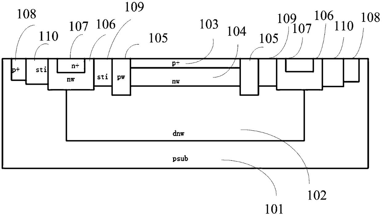
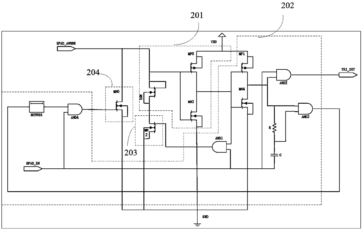
[0023] The idea of ​​this application is: on the original single photon avalanche diode SPAD structure, add the protection ring of deep N well and STI layer, and combine the active quenching circuit with feedback, which can reduce the edge electric field and central electric field, and improve the reverse strike The breakdown voltage avoids the premature breakdown of the diode, thereby improving the detection efficiency. This method has a fast quenching speed, a high photon count rate, and a small post-pulse effect.

[0024] see figure 1 , the present application proposes a single photon avalanche diode SPAD, the single photon avalanche diode SPAD includes: P-type substrate 101, deep N well 102, first P+ ion region 103, first N well region 104, P well region 105, the first Two N well regions 106 , a first N+ ion region 107 , a ...


PUM


Abstract

The present application provides a single-photon avalanche diode, an active quenching circuit, a pulsed TOF sensor, and a forming method for the single-photon avalanche diode. The single photon avalanche diode includes a P-type substrate; a deep n-well formed above the P-type substrate; a first N-well region which is formed above the deep n-well; a first P+ ion region which is formed above the first N-well region; a P-well region which surrounds the first N-well region and the first P+ ion region and is disposed deep n-well; a second N-well region which is disposed in the deep n-well around the P-well region, and extends onto the P-type substrate; a first N+ ion region formed in the second N-well region; and a second P+ ion region disposed on the P-type substrate around the second N-well region. The method can increase the reverse breakdown voltage, and avoids the early breakdown of a diode, thereby improving the detection efficiency, speeding up the avalanche effect of a completely quenched device, and preventing the single-photon avalanche diode from being triggered again during the restoration of the detection state.

Description

technical field [0001] The present application relates to the field of sensors, in particular to a single photon avalanche diode, an active quenching circuit, a pulsed TOF sensor and a method for forming the single photon avalanche diode. Background technique [0002] The research situation at home and abroad on SPAD (Single Photon Avalanche Diode, single photon diode) depth image is as follows. Foreign research status: In 1998, Lincoln Laboratory integrated the readout circuit and Gm-APD (Avalanche Photondiode) array on the same substrate for the first time, and produced a 4×4 Gm-APD array. In 2002, Lincoln Laboratory announced the manufacture of a detection chip composed of 1024 Gm-APDs, which uses bridge integration technology and can perform single-photon detection under extremely weak light conditions. In 2005, Cristiano Niclass and others successfully manufactured a 32×32 SPAD depth image sensor on the standard 0.8μm CMOS (Complementary Metal-Oxide-Semiconductor) proc...

Claims


Application Information

Patent Timeline
IPC IPC(8): H01L31/14
CPCH01L31/143
Inventor 徐渊王育斌陈享陈志芳潘安黄志宇
Owner SHENZHEN TECH UNIV
Learn More