Supercharge Your Innovation With Domain-Expert AI Agents!

Phosphorescent main compound and organic light-emitting device using compound

A phosphorescent subject and compound technology, applied in the field of organic electroluminescent devices, can solve the problems of complicated manufacturing process, increased production cost, and lack of solubility, etc., and achieve the effects of prolonged durability, excellent color purity and brightness

Inactive Publication Date: 2019-03-22
ZHEJIANG HUADISPLAY OPTOELECTRONICS CO LTD
View PDF4 Cites 5 Cited by
  • Summary
  • Abstract
  • Description
  • Claims
  • Application Information

AI Technical Summary

Problems solved by technology

However, these compounds do not have ideal solubility in solvents and thus cannot be used to form the light-emitting layer by solution process
The light-emitting layer should be formed by a deposition process, so the manufacturing process is extremely complicated and the process efficiency is extremely low
In addition, the waste in the deposition process is very high, resulting in increased production costs

Method used


Image

  • Phosphorescent main compound and organic light-emitting device using compound
  • Phosphorescent main compound and organic light-emitting device using compound
  • Phosphorescent main compound and organic light-emitting device using compound

Examples


no. 1 approach

[0100] The ITO glass substrate was patterned to have a light emitting area of ​​3 mm x 3 mm. Then, the patterned ITO glass substrate was washed.

[0101] The substrate is then placed in a vacuum chamber. The standard pressure setting is 1×10 -6 support. After that, on the ITO substrate with

[0102] and The sequence forms layers of organic matter.

[0103] At 0.9mA, the brightness is equal to 1263cd / m 2 (5.6V). At this time, CIEx=0.659, y=0.330.

no. 2 approach

[0105] The ITO glass substrate was patterned to have a light emitting area of ​​3 mm x 3 mm. Then, the patterned ITO glass substrate was washed.

[0106] The substrate is then placed in a vacuum chamber. The standard pressure setting is 1×10 -6 support. After that, on the ITO substrate with

[0107] and The sequence forms layers of organic matter.

[0108] At 0.9mA, the brightness is equal to 1172cd / m 2 (5.8V). At this time, CIEx=0.660, y=0.329.

no. 3 approach

[0110] The ITO glass substrate was patterned to have a light emitting area of ​​3 mm x 3 mm. Then, the patterned ITO glass substrate was washed.

[0111] The substrate is then placed in a vacuum chamber. The standard pressure setting is 1×10 -6 support. After that, on the ITO substrate with

[0112] and The sequence forms layers of organic matter.

[0113] At 0.9mA, the brightness is equal to 1281cd / m 2 (5.7V). At this time, CIEx=0.659, y=0.329.


PUM

PropertyMeasurementUnit
luminanceaaaaaaaaaa

Abstract

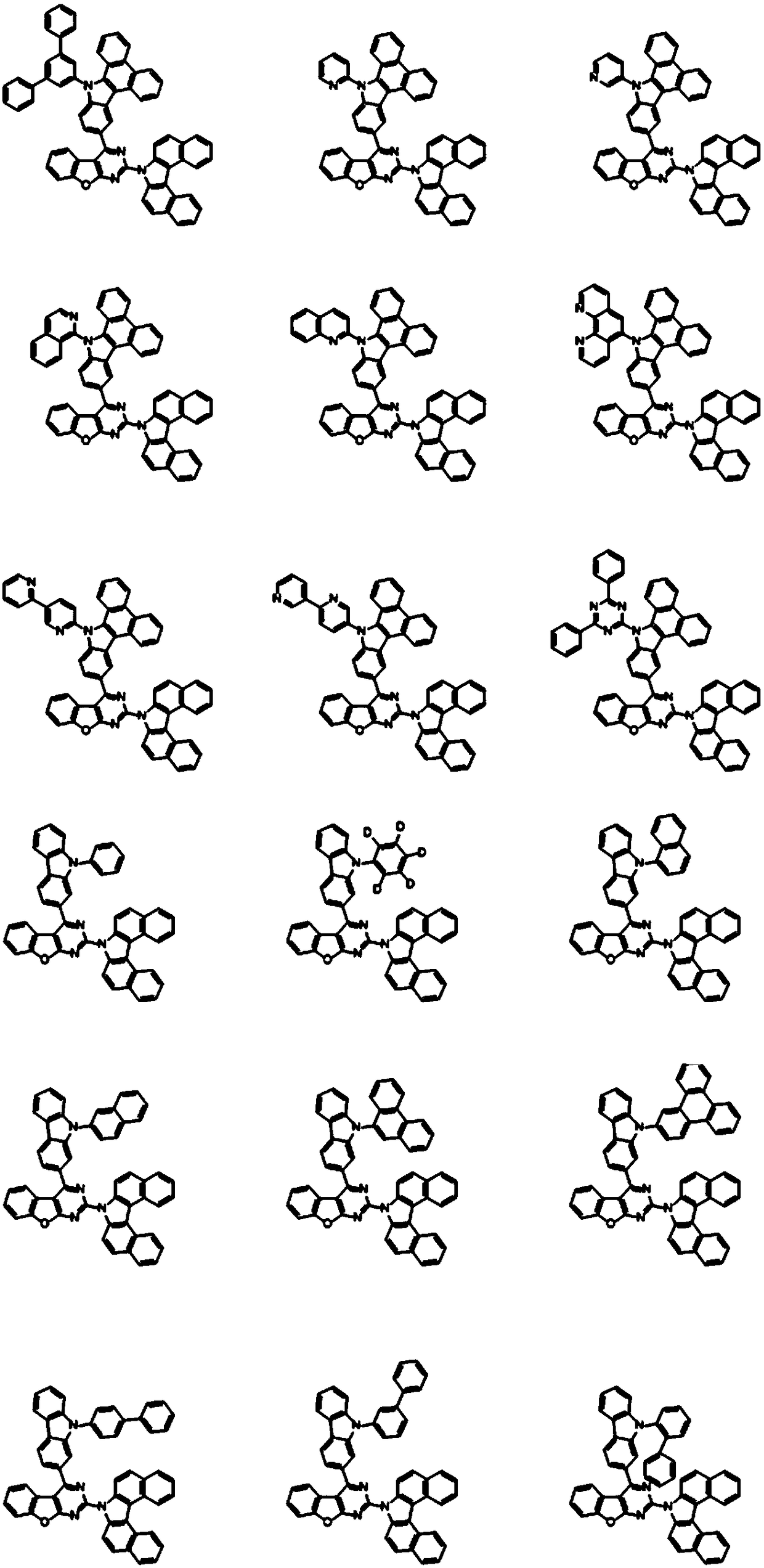
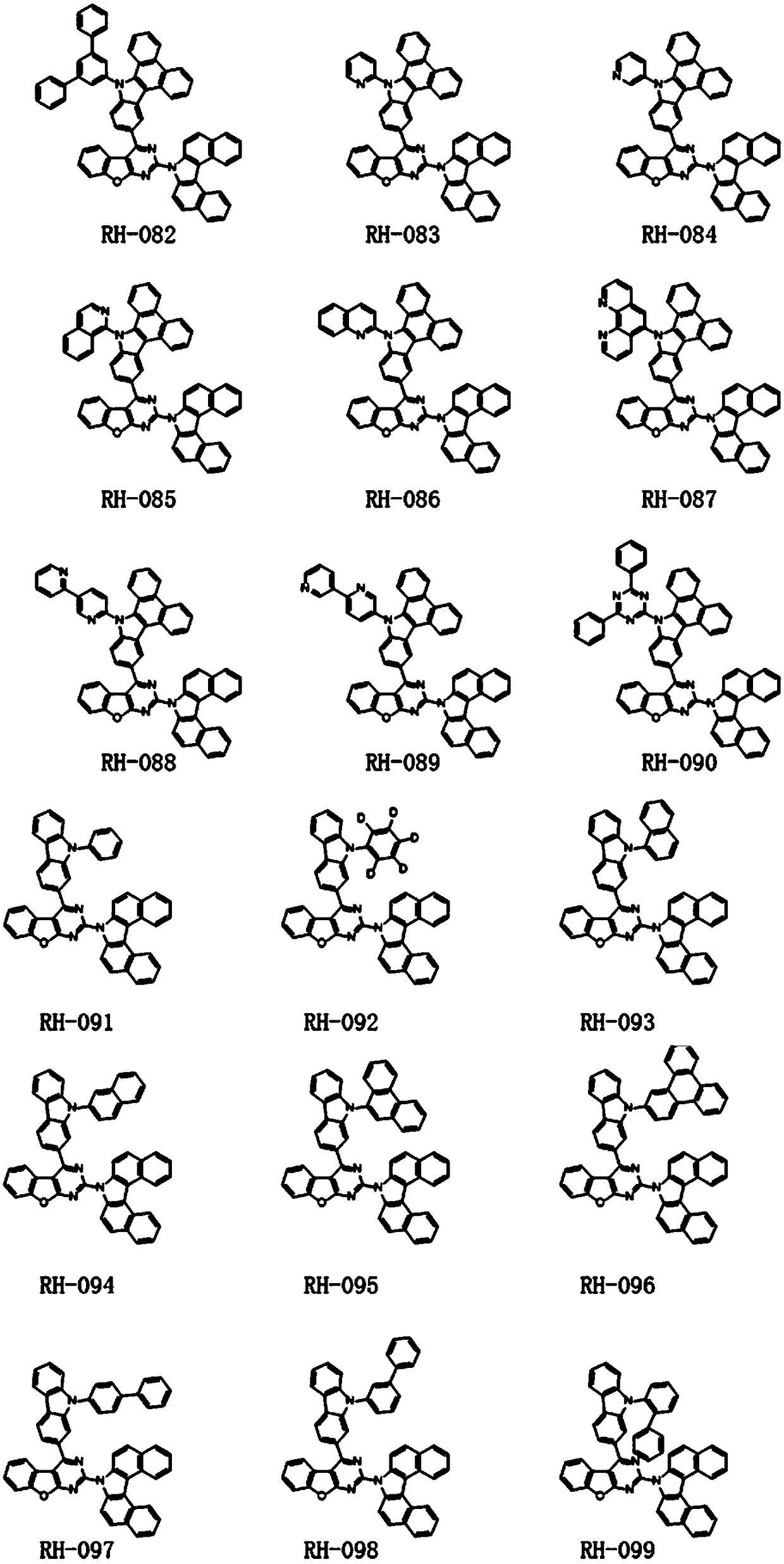
The invention relates to a phosphorescent main compound and an organic light-emitting device using the compound. The structural formula of the phosphorescent main compound is shown as formula I; in the structural formula I, X is or S; Z is independently selected from the following structures; Ar is independently selected from one of C6-C30 aryl and C2-C30 hetero-aryl. According to the invention, when the chemical formula shown as formula I is used as a main material of an illuminating layer of an organic light emitting diode (organic light-emitting device), color purity and brightens are excellent and durability is promoted.

Description

technical field [0001] The present invention relates to a phosphorescent host compound and an organic electroluminescent device using the compound. Background technique [0002] Recently, demand for flat panel displays such as liquid crystal displays and plasma display panels is increasing. However, these flat panel displays have slower response times and narrower viewing angles than cathode ray tubes (CRTs). [0003] Organic Light Emitting Diode (OLED) devices are one of the next-generation flat panel displays that can solve the above problems and occupy a smaller footprint. [0004] Components of OLED devices can be formed on flexible substrates, such as plastic substrates. In addition, OLED devices have advantages in viewing angle, driving voltage, power consumption, and color purity. On the other hand, OLED devices are powerful enough to produce full-color images. [0005] Generally, a light emitting diode of an OLED device includes an anode, a hole injection layer (...

Claims


Application Information

Patent Timeline
Patent Type & Authority Applications(China)
IPC IPC(8): C07D491/048C07D495/04C07D519/00C09K11/06H01L51/54
CPCC09K11/06C07D491/048C07D495/04C07D519/00C09K2211/1044C09K2211/1059C09K2211/1092C09K2211/1088C09K2211/1011C09K2211/1007C09K2211/1029H10K85/615H10K85/654H10K85/657H10K85/6572
Inventor 郑贤哲黄东华万鸣全美子赵晓宇
Owner ZHEJIANG HUADISPLAY OPTOELECTRONICS CO LTD
Features
  • R&D
  • Intellectual Property
  • Life Sciences
  • Materials
  • Tech Scout
  • Unparalleled Data Quality
  • Higher Quality Content
  • 60% Fewer Hallucinations
Learn More