Display module and forming method thereof

A display module and display panel technology, which is applied in character and pattern recognition, instruments, printing image acquisition, etc., can solve the problems of loss of display module yield, difficulty in ensuring the production yield of display module, and large thickness, etc., to achieve High yield, small thickness, and the effect of reducing yield loss

Inactive Publication Date: 2019-03-22
SHANGHAI OXI TECH
View PDF4 Cites 5 Cited by
  • Summary
  • Abstract
  • Description
  • Claims
  • Application Information

AI Technical Summary

Problems solved by technology

[0005] However, the thickness of the display module with fingerprint recognition function is often relatively large, and the existing thinning process w

Method used


Image

  • Display module and forming method thereof
  • Display module and forming method thereof
  • Display module and forming method thereof

Examples


Embodiment Construction

[0048] It can be seen from the background technology that the existing display modules with fingerprint recognition function are often thicker, and the existing thinning process will cause a high yield loss in the manufacturing process, making it difficult to achieve manufacturing yield and module thinning take into account.

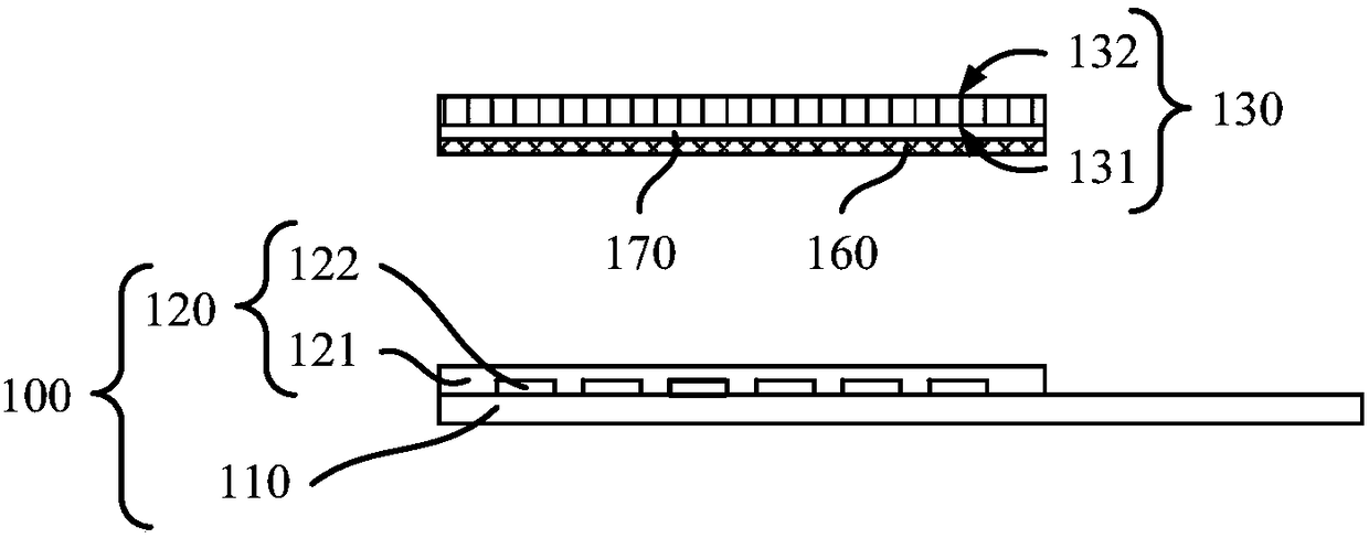
[0049] In order to solve the above-mentioned technical problems, the present invention provides a display module and its forming method, by directly forming a device layer on a flexible plastic substrate to form an optical sensor; then integrating a self-luminous display panel and protection on the optical sensor layer. The use of the flexible plastic substrate can achieve both high yield and small thickness.

[0050] In order to make the above objects, features and advantages of the present invention more comprehensible, specific embodiments of the present invention will be described in detail below in conjunction with the accompanying drawings.

[00...


PUM

PropertyMeasurementUnit
Thicknessaaaaaaaaaa
Thicknessaaaaaaaaaa
Thicknessaaaaaaaaaa

Abstract

A display module and a forming method thereof, the forming method comprising: providing a flexible plastic substrate; Forming a device layer on the flexible plastic substrate, the device layer and theflexible plastic substrate for forming an optical sensor; Providing a protective cover plate and a self-luminescent display panel located on the surface of the protective cover plate; oppositely attaching The self-luminescent display panel and the optical senso. A device layer is directly formed on a flexible plastic substrate to form an optical sensor, so as to achieve the purpose of giving consideration to both high yield and small thickness.

Description

technical field [0001] The invention relates to the field of optical fingerprint identification, in particular to a display module and a forming method thereof. Background technique [0002] Fingerprint imaging recognition technology is to collect the fingerprint image of the human body through the fingerprint sensor, and then compare it with the existing fingerprint imaging information in the system to judge whether it is correct or not, and then realize the technology of identity recognition. Due to its ease of use and the uniqueness of human fingerprints, fingerprint recognition technology has been widely used in various fields. For example, security inspection areas such as public security bureaus and customs, building access control systems, and consumer products such as personal computers and mobile phones, etc. [0003] The realization of fingerprint imaging recognition technology includes optical imaging, capacitive imaging, ultrasonic imaging and other technologies...

Claims


Application Information

Patent Timeline
IPC IPC(8): G06K9/00G06K9/20
CPCG06V40/1324G06V40/1318G06V10/94G06V10/145
Inventor 凌严朱虹
Owner SHANGHAI OXI TECH
Why Eureka
Try Eureka