Epitaxial wafer of light emitting diode, and preparation method thereof

A technology of light-emitting diodes and epitaxial wafers, which is applied in the direction of electrical components, circuits, semiconductor devices, etc., can solve problems affecting the crystal quality of GaN layers, affecting the crystal quality of epitaxial wafers, and multi-lattice, so as to reduce lattice defects and merge The effect of reducing the number of times and improving the crystal quality

Inactive Publication Date: 2019-03-22
HC SEMITEK ZHEJIANG CO LTD
View PDF5 Cites 1 Cited by
  • Summary
  • Abstract
  • Description
  • Claims
  • Application Information

AI Technical Summary

Problems solved by technology

However, the island structure will produce more lattice defects during the merging process, which will affect the crystal quality of the undoped GaN layer, and then affect the overall crystal quality of the epitaxial wafer.

Method used


Image

  • Epitaxial wafer of light emitting diode, and preparation method thereof
  • Epitaxial wafer of light emitting diode, and preparation method thereof
  • Epitaxial wafer of light emitting diode, and preparation method thereof

Examples


Embodiment Construction

[0029] In order to make the object, technical solution and advantages of the present invention clearer, the implementation manner of the present invention will be further described in detail below in conjunction with the accompanying drawings.

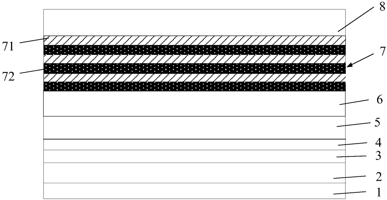
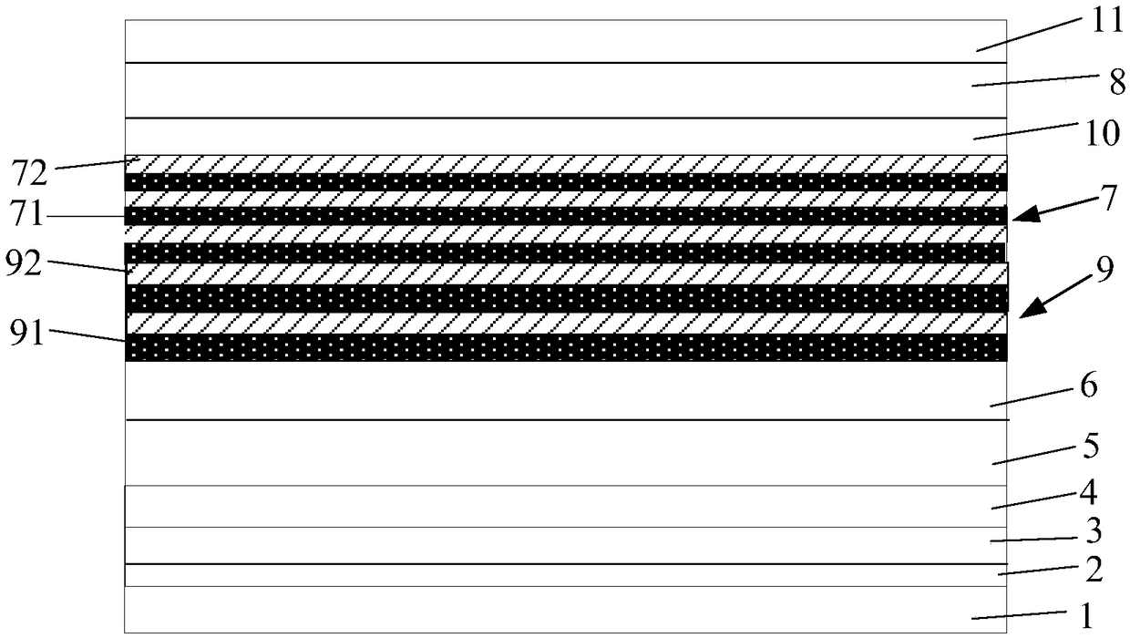
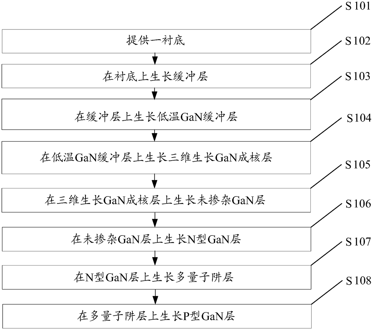
[0030] figure 1 It is a schematic structural diagram of an epitaxial wafer of a light emitting diode provided by an embodiment of the present invention, as shown in figure 1 As shown, the epitaxial wafer includes a substrate 1, a buffer layer 2, a low-temperature GaN buffer layer 3, a three-dimensionally grown GaN nucleation layer 4, an undoped GaN layer 5, and an N-type GaN layer 6 sequentially stacked on the substrate 1. , the multi-quantum well layer 7 and the P-type GaN layer 8, wherein the three-dimensionally grown GaN nucleation layer 4 is doped with Mg element.

[0031] Doping Mg element in the three-dimensional growth GaN nucleation layer 4, because the viscosity coefficient of Mg atoms is large and the mobility is low, the Mg...


PUM


Abstract

The invention discloses an epitaxial wafer of a light emitting diode, and a preparation method thereof, which belong to the field of light emitting diode manufacturing. The Mg element is doped in a three-dimensionally grown GaN nucleation layer, since the viscosity coefficient of Mg atoms is large and the mobility is low, the Mg atoms on an island structure can aggregate gallium atoms and nitrogenatoms well when the three-dimensionally grown GaN nucleation layer is growing, such that the size of the island structure is increased, the generated island structure is more prone to absorb atoms due to the doped Mg element, surrounding new island structures are difficult to form, finally a number of island structures which can be formed on a low-temperature GaN buffer layer is reduced, the distance between the island structures is greater, the size of the island structure is increased while the density of the island structures on the low-temperature GaN buffer layer is smaller, a number ofcombination times of the island structures is reduced, further the lattice defect occurred in the combining process of the island structures can be reduced, the crystal quality of the undoped GaN layer is improved, and the overall crystal quality of the epitaxial wafer is improved.

Description

technical field [0001] The invention relates to the field of light-emitting diode manufacturing, in particular to an epitaxial wafer of a light-emitting diode and a preparation method thereof. Background technique [0002] Light-emitting diodes are semiconductor diodes that can convert electrical energy into light energy. They have the advantages of small size, long life, and low power consumption. They are currently widely used in automotive signal lights, traffic lights, display screens, and lighting equipment. The epitaxial wafer is the basic structure for making light-emitting diodes. The structure of the epitaxial wafer includes a substrate and a buffer layer grown on the substrate in turn, a low-temperature GaN buffer layer, a three-dimensionally grown GaN nucleation layer, an undoped GaN layer, and an N-type GaN layer. layer, multi-quantum well layer and P-type GaN layer. [0003] The three-dimensionally grown GaN nucleation layer includes a plurality of island struc...

Claims


Application Information

Patent Timeline
Patent Type & Authority Applications(China)
IPC IPC(8): H01L33/32H01L33/12H01L33/00
CPCH01L33/325H01L33/0066H01L33/0075H01L33/12
Inventor 丁杰秦双娇胡任浩周飚胡加辉
Owner HC SEMITEK ZHEJIANG CO LTD
Why Eureka
Try Eureka