

TSV array temperature optimization method based on an orthogonal test
A technology of orthogonal test and optimization method, applied in the field of microelectronics, can solve the problems of low accuracy, large workload, poor general applicability, etc., to improve efficiency and accuracy, reduce required time, avoid comprehensive testing and The effect of random error
- Summary
- Abstract
- Description
- Claims
- Application Information
AI Technical Summary
Problems solved by technology
Method used
Image

Examples
Embodiment Construction
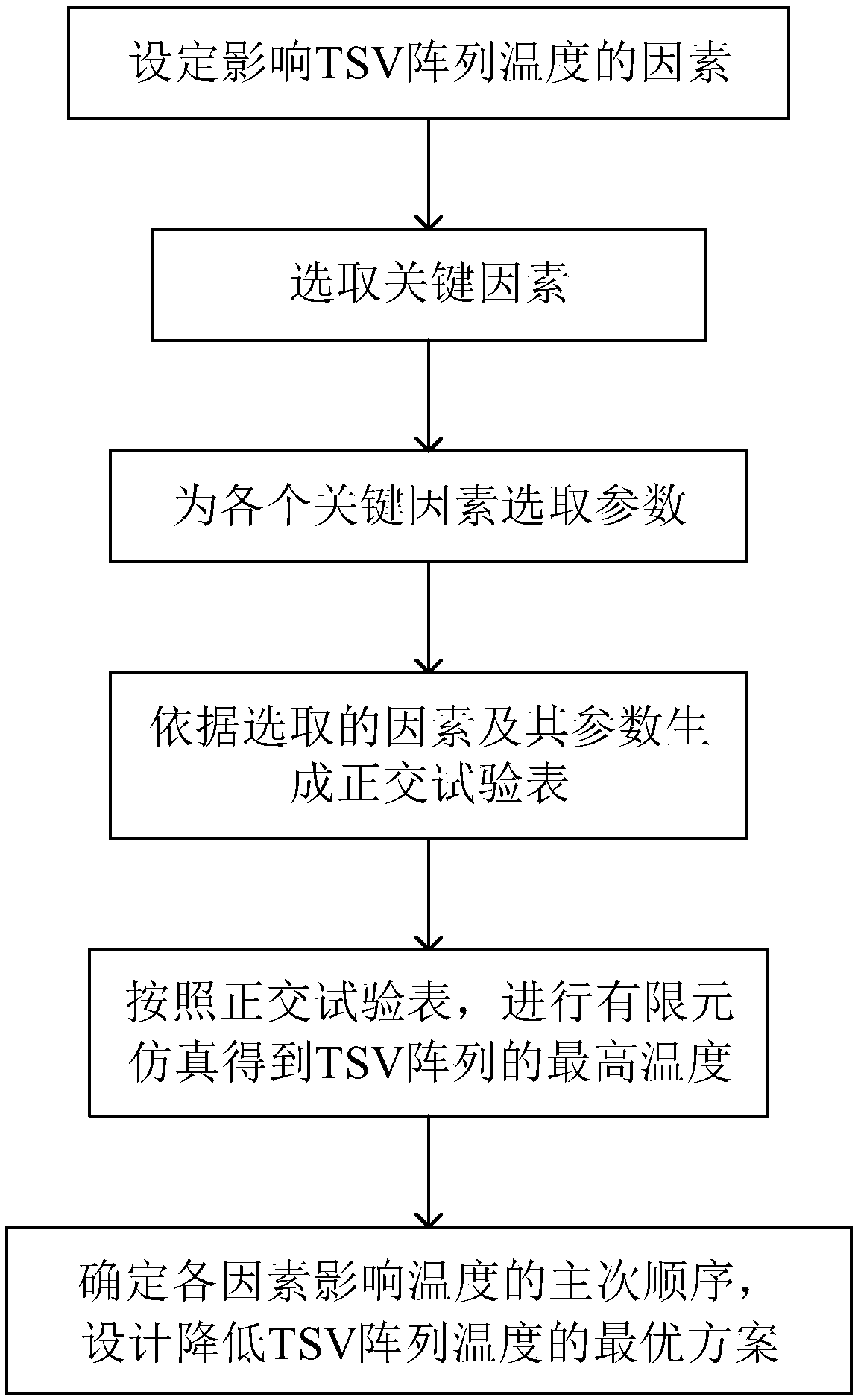
[0023] Embodiments and effects of the present invention will be described in further detail below with reference to the accompanying drawings.
[0024] refer to figure 1 , the present invention is based on the orthogonal experiment TSV array temperature optimization method, the implementation steps are as follows:
[0025] Step 1. Set the factors that affect the temperature of the TSV array.
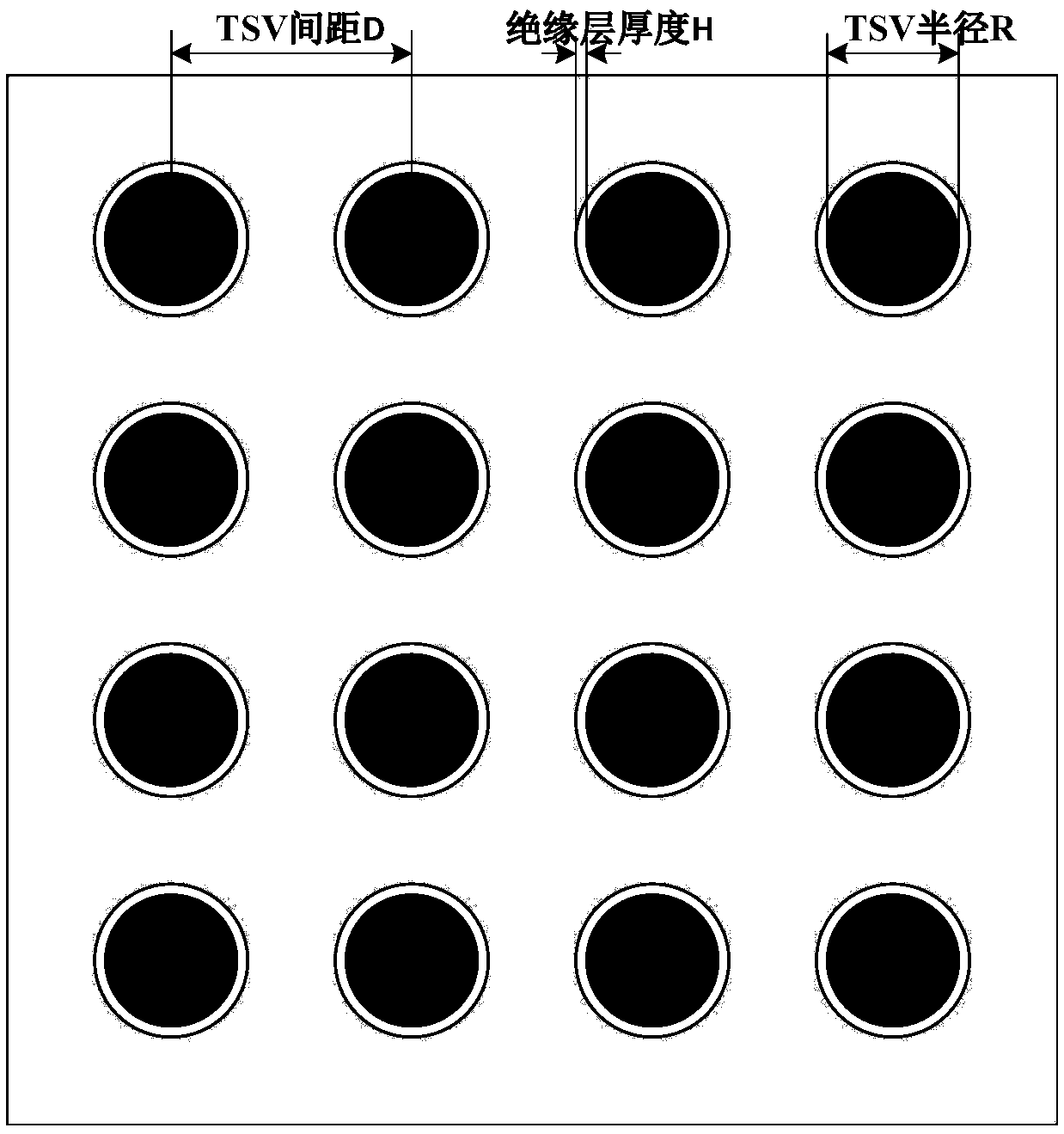
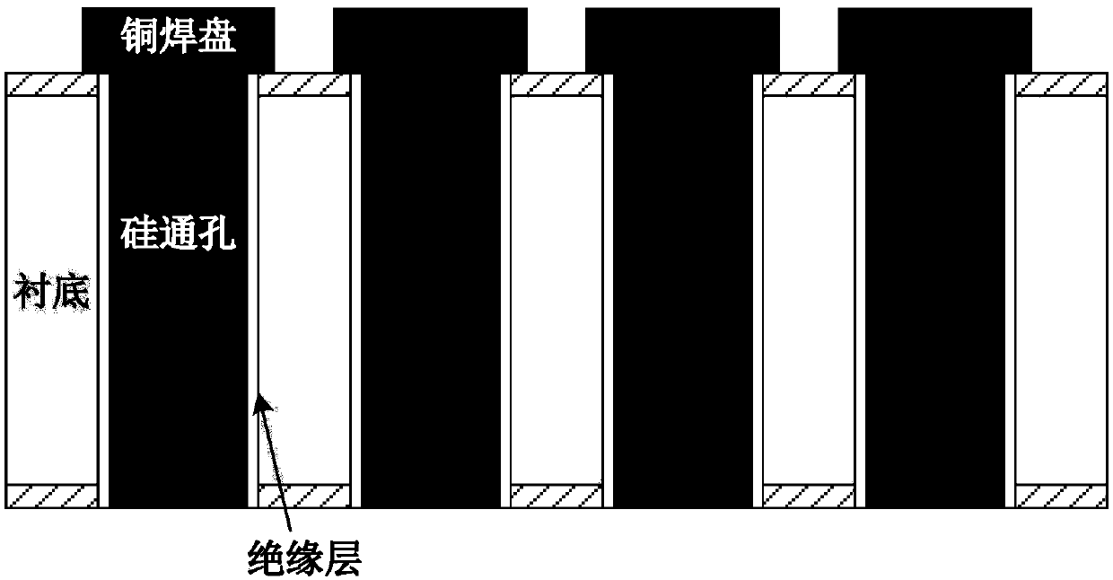
[0026] The set factors include: hole category C, radius R, spacing D, filling material M tsv , arrangement S, insulating layer thickness H and insulating layer material M iso .
[0027] Step 2. Select the key factors affecting the temperature of the TSV array.
[0028] Select at least three factors from the factors that affect the temperature of the TSV array as the key factors. The number of key factors selected in this example is four, namely, the radius R of the TSV, the spacing D of the TSV, the thickness H of the insulating layer, and the material of the insulating layer. m is...
PUM
| Property | Measurement | Unit |
|---|---|---|
| Height | aaaaa | aaaaa |
| Radius | aaaaa | aaaaa |
| Height | aaaaa | aaaaa |
Abstract
Description
Claims
Application Information