A passive optical interconnection network structure

A network structure, passive optical technology, applied in electrical components, selection devices of multiplexing systems, selection devices, etc., can solve the problems of optical network communication blockage and large loss, etc.

Active Publication Date: 2021-09-14
XIAN UNIV OF POSTS & TELECOMM
View PDF7 Cites 0 Cited by
  • Summary
  • Abstract
  • Description
  • Claims
  • Application Information

AI Technical Summary

Problems solved by technology

[0004] The present invention provides a passive optical interconnection network structure, which solves the problems of blockage and large loss of optical network communication during large-scale expansion

Method used


Image

  • A passive optical interconnection network structure
  • A passive optical interconnection network structure
  • A passive optical interconnection network structure

Examples


Embodiment Construction

[0036] In order to better explain the present invention and facilitate understanding, the present invention will be described in detail below through specific embodiments in conjunction with the accompanying drawings.

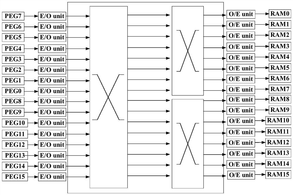
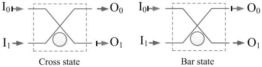
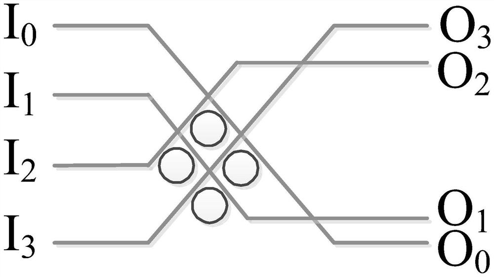
[0037] The passive optical interconnection network is an important structural transmission mode for the on-chip optical interconnection. The wavelength division multiplexing technology can realize the synthesis and splitting of wavelengths to meet the scalability of the on-chip optical interconnection network. Passive on-chip optical interconnection network can have higher bandwidth, faster speed and lower energy consumption. In the case of small-scale circuits, the advantages of optical interconnection are not obvious compared with traditional electrical interconnection methods. However, with the further development of technology, communication between larger and more complex circuits has a significant impact on transmission speed, bandwidth, The requirements ...


PUM


Abstract

The invention relates to a passive optical interconnection network structure. The passive optical interconnection network structure includes: two-stage optical switching switches; wherein, the two-stage optical switching switches respectively receive read / write request optical signals sent by N processing elements; according to the read / write request optical signals in the Wavelength information is exchanged to realize non-blocking parallel access among 16 processing elements; N is 4*4, 8*8, 16*16, 32*32 or 64*64. The invention relates to an on-chip passive optical interconnection network structure, which is suitable for communication of a large-scale multi-core processing unit structure, and aims to reduce the number of microring resonators and improve Access bandwidth, lower insertion loss, and lower access latency.

Description

technical field [0001] The invention belongs to the technical field of integrated circuit design, and in particular relates to a passive optical interconnection network structure. Background technique [0002] With the development of multi-core processors, on-chip optical interconnection has become an important communication structure. Compared with electrical interconnect structures, passive optical interconnect structures have higher bandwidth, faster speed and lower loss. At present, the integrated chip of photonic elements and transistors has been realized, and the photonic devices on the chip are used to communicate directly with other chips to achieve optical communication between chips. [0003] The transmission path of the on-chip optical interconnection network structure, the optical interconnection network structure and the receiving path are important components of communication. However, in the traditional active cross-waveguide double microring resonator optic...

Claims


Application Information

Patent Timeline
Patent Type & Authority Patents(China)
IPC IPC(8): H04Q11/00
CPCH04Q11/0005H04Q11/0067H04Q2011/0086
Inventor 山蕊吴皓月蒋林邓军勇刘有耀朱筠贺飞龙
Owner XIAN UNIV OF POSTS & TELECOMM
Why Eureka
Try Eureka