Manufacturing method of magnetic radom access memory unit array and peripheral circuit connecting wires

A technology of random access memory and cell array, which is applied in semiconductor/solid-state device manufacturing, circuits, electrical components, etc. It can solve the problems of MRAM device pollution, time-related dielectric breakdown, damage, etc., and achieve the effect of optimizing and improving electrical performance

Inactive Publication Date: 2019-03-29
SHANGHAI CIYU INFORMATION TECH CO LTD
View PDF4 Cites 6 Cited by
  • Summary
  • Abstract
  • Description
  • Claims
  • Application Information

AI Technical Summary

Problems solved by technology

However, since the size of the MTJ structural unit is smaller than that of the VIA x (x>=1) The size of the top opening is small. When etching the magnetic tunnel junction and its bottom electrode, in order to completely isolate the MTJ units, over-etching must be carried out. In the over-etching, the magnetic tunnel junction is not blocked. and its bottom electrode covered copper VIA x (x>=1) area will be partially etched and also damage its diffusion barrier layer (Ta / TaN), which will form copper VIA x (x>=1) to the diffusion channel of the low-k dielectric outside it, Cu atom will be diffused in the low-k dielectric, and this is bound to affect the electrical performance of MRAM, such as: time-dependent dielectric breakdown (TDDB , TimeDependent Dielectric Breakdown) and electron mobility (EM, Electron Mobility), etc., causing damage
[0006]In addition, during the over-etching process of the magnetic tunnel junction and its bottom electrode, due to ion bombardment (IonBombardment), copper atoms and their forming compounds will be sputtered into the The sidewall of the magnetic tunnel junction and the surface of the etched low-k material, thereby contaminating the entire MRAM device

Method used


Image

  • Manufacturing method of magnetic radom access memory unit array and peripheral circuit connecting wires
  • Manufacturing method of magnetic radom access memory unit array and peripheral circuit connecting wires
  • Manufacturing method of magnetic radom access memory unit array and peripheral circuit connecting wires

Examples


Embodiment example 1

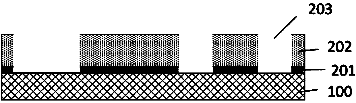
[0037] Step 1: Provide surface finish with metal connection (M x (x>=1) CMOS substrate 100, on which bottom electrode via holes (BEV, Bottom Electrode Via) 203 are formed, and then non-copper metal filling is performed.

[0038] Further, step 1 can be divided into the following forming steps:

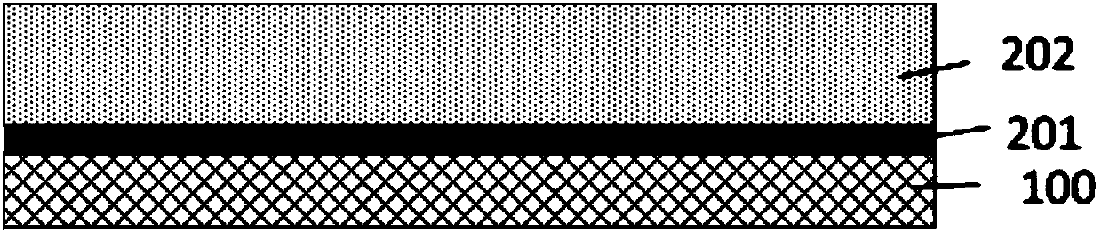
[0039] Step 1.1: Deposit a diffusion barrier layer 201 and a bottom electrode via dielectric 202, as shown in FIG. x ), the diffusion protection layer of copper to the bottom electrode through-hole dielectric 202 can also be used as an etching barrier layer for BEV etching, with a thickness of 10nm-50nm, and the forming material can be SiN, SiC or SiCN. The thickness of the bottom electrode through-hole dielectric 202 is 60nm-150nm, and the forming material can be SiO 2 , SiON or low-k, etc.; wherein, the low dielectric constant (low-k) dielectric refers to a material with a dielectric constant (k) lower than that of silicon dioxide (k=3.9).

[0040] Wherein, the low dielectric const...

Embodiment example 2

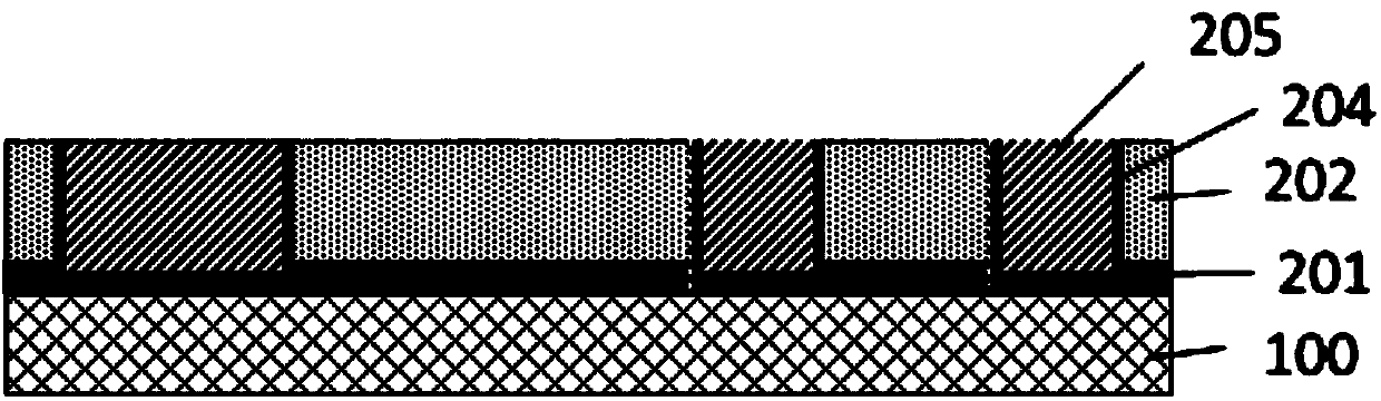
[0075] Since BEV is not Cu metal, BEC can also grow together with MTJ multilayer film, or even omit BEC, and use the same MTJ mask, and then use self-alignment to etch MTJ and BEC successively, because BEV uses non-Cu metal , so it doesn't matter that the BEV surface is exposed during the etching process. This saves several steps.

[0076] Compared with the first embodiment, in the second embodiment, no bottom electrode contact is made. The steps are as follows:

[0077] Step 1: Same as Step 1 of Implementation Case 1, such as Figure 1(a)-Figure 1(c) shown;

[0078] Step 2: Same as Step 3 of Implementation Case 1, such as Figure 3(a)-Figure 3(c) shown;

[0079] Step 3: Same as Step 4 of Implementation Case 1, such as Figure 3(d)-Figure 3(h) shown.


PUM


Abstract

The invention provides a manufacturing method of a magnetic radom access memory unit array and peripheral circuit connecting wires. The manufacturing method comprises the steps of: (1) providing a surface-polished CMOS substrate with metal connecting wires, forming bottom electrode vias in the substrate, and then filling the bottom electrode vias with non-copper metal; (2) making bottom electrodecontact on the bottom electrode vias; (3) manufacturing a magnetic tunnel junction structural unit on the bottom electrode contact; (4) and forming top electrode vias in the magnetic tunnel junction structural unit, and manufacturing metal connecting wires realizing connection with a logic / memory unit. The non-copper metal is selected from one of Ta, TaN, Ti, TiN, W or WN. Since the magnetic tunnel junction is manufactured on and its bottom electrodes can be formed in the metal of the surface-polished non-copper bottom electrode vias, the copper contamination and copper diffusion caused by directly manufacturing the MTJ on the copper Vx(x>=1) are effectively avoided, thereby being very conductive to the optimization and improvement of electrical performance of an MRAM loop and the miniaturization of the device.

Description

technical field [0001] The invention relates to a manufacturing method of a magnetic random access memory (MRAM) unit array and peripheral circuit wiring, and belongs to the technical field of magnetic random access memory (MRAM, Magnetic Radom Access Memory) manufacturing. Background technique [0002] In recent years, MRAM using magnetic tunnel junction (MTJ) has been considered as the future solid-state non-volatile memory, which has the characteristics of high-speed reading and writing, large capacity and low energy consumption. Ferromagnetic MTJ is usually a sandwich structure, which has a magnetic memory layer, which can change the magnetization direction to record different data; an insulating tunnel barrier layer in the middle; a magnetic reference layer, located on the other side of the tunnel barrier layer, which The direction of magnetization remains unchanged. [0003] In order to record information in this magnetoresistive element, it is suggested to use a writ...

Claims


Application Information

Patent Timeline
Patent Type & Authority Applications(China)
IPC IPC(8): H01L21/82H01L27/22
CPCH01L21/82H10B61/22
Inventor 肖荣福张云森郭一民陈峻
Owner SHANGHAI CIYU INFORMATION TECH CO LTD
Why Eureka
Try Eureka