Etching method of organic film and repairing method of display area circuit of display substrate

A technology of display substrate and display area, applied in circuits, electrical components, electrical solid devices, etc., can solve problems such as speeding up the etching speed, and achieve the effect of speeding up the etching speed, solving the etching damage, and ensuring the etching effect

Active Publication Date: 2021-10-26
BOE TECH GRP CO LTD +1
View PDF10 Cites 0 Cited by
  • Summary
  • Abstract
  • Description
  • Claims
  • Application Information

AI Technical Summary

Problems solved by technology

In the etching method of the organic film, water vapor is fed to the surface to be etched during the process of etching the organic film by the focused ion beam, so that the position to be etched of the organic film can be etched quickly in a targeted manner, and the During the etching process, it will not cause etching damage to other non-etching positions of the organic film, thereby solving the problem that the non-etching position is damaged by the etching caused by the existing concentrated sulfuric acid etching, and also speeding up the etching process speed

Method used


Image

  • Etching method of organic film and repairing method of display area circuit of display substrate
  • Etching method of organic film and repairing method of display area circuit of display substrate
  • Etching method of organic film and repairing method of display area circuit of display substrate

Examples


Embodiment 1

[0037] This embodiment provides an etching method for an organic film, which includes etching the position to be etched of the organic film through a focused ion beam, and during the etching process, the to-be-etched surface of the position to be etched of the organic film is into water vapor.

[0038] Wherein, the etching of the organic film is carried out in a real-time vacuum environment.

[0039] The high-energy focused ion beam can make the originally inactive water vapor active, and the active water vapor can react with the organic film to generate volatile substances, which can be pumped out with the real-time vacuum system during the etching process. Outside the etching environment, by injecting water vapor onto the surface to be etched during the process of etching the organic film by the focused ion beam, the position to be etched of the organic film can be etched quickly in a targeted manner, and during the etching process It does not cause etching damage to other ...

Embodiment 2

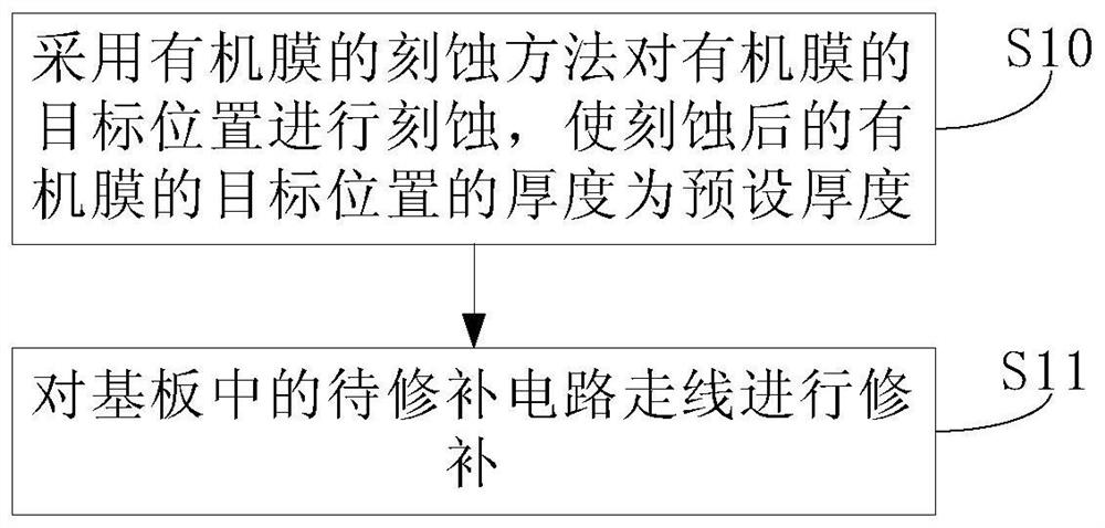
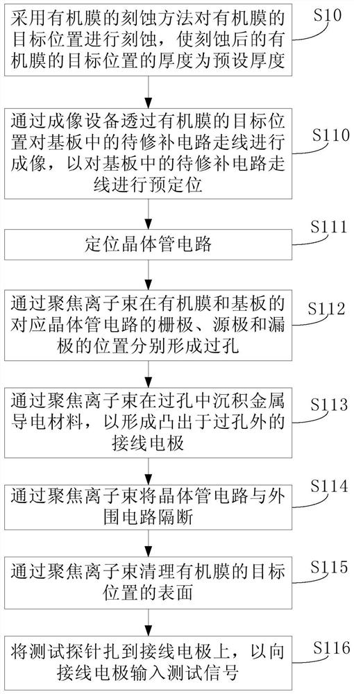
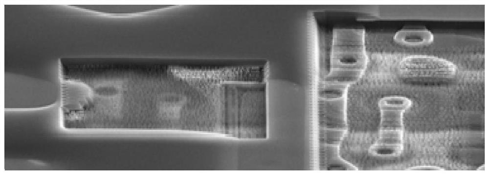
[0045] This embodiment provides a method for repairing the circuit in the display area of ​​the display substrate. The display substrate includes a substrate and an organic film disposed on the substrate. The substrate is provided with circuit traces corresponding to the display area, and the organic film covers the circuit traces. to protect circuit traces, such as figure 1 with figure 2 As shown, the repairing method includes: Step S10: using the organic film etching method in Embodiment 1 to etch the target position of the organic film, so that the thickness of the target position of the organic film after etching is a preset thickness. Step S11: repairing the wiring of the circuit to be repaired in the substrate. The location of the circuit trace to be repaired corresponds to the location of the target location.

[0046] Wherein, the display substrate includes an organic electroluminescent display substrate. Repairing the circuit traces to be repaired in the substrate in...


PUM


Abstract

The invention provides an etching method of an organic film and a repairing method of a circuit in a display area of ​​a display substrate. The etching method of the organic film includes etching the position to be etched of the organic film by means of a focused ion beam; In the etching method of the organic film, water vapor is fed to the surface to be etched during the process of etching the organic film by the focused ion beam, so that the position to be etched of the organic film can be etched quickly in a targeted manner, and the During the etching process, it will not cause etching damage to other non-etching positions of the organic film, thereby solving the problem of non-etching positions being damaged by etching caused by the existing concentrated sulfuric acid etching, and also speeding up the etching process. speed.

Description

technical field [0001] The invention relates to the field of display technology, in particular to an etching method of an organic film and a repair method of a circuit in a display area of ​​a display substrate. Background technique [0002] Due to the advantages of high contrast, wide color gamut, fast response speed, and bendability, flexible OLED display panels are increasingly used in smart display terminals and become the next-generation display technology. [0003] The flexible OLED display panel is made up of multi-layer thin films. Since the TFT pixel drive circuit is located at the bottom of the substrate, it is impossible to directly test the electrical characteristics of the TFT in the display area. It is necessary to test the electrical characteristics of the TFT fabricated in the edge area of ​​the panel, and then The electrical properties of the TFTs in the display area are inferred from the electrical properties of the TFTs in the panel edge area. However, du...

Claims


Application Information

Patent Timeline
Patent Type & Authority Patents(China)
IPC IPC(8): H01L51/56
CPCH10K59/1201H10K71/00
Inventor 包征范磊辛燕霞
Owner BOE TECH GRP CO LTD
Why Eureka
Try Eureka