Solid-state imaging device and method for manufacturing same
A camera device and solid-state image technology, applied in image communication, radiation control devices, electric solid-state devices, etc., can solve problems such as image quality deterioration, achieve the effects of improving sensitivity, ensuring area, and suppressing image quality degradation
- Summary
- Abstract
- Description
- Claims
- Application Information
AI Technical Summary
Problems solved by technology
Method used
Image

Examples
no. 1 approach
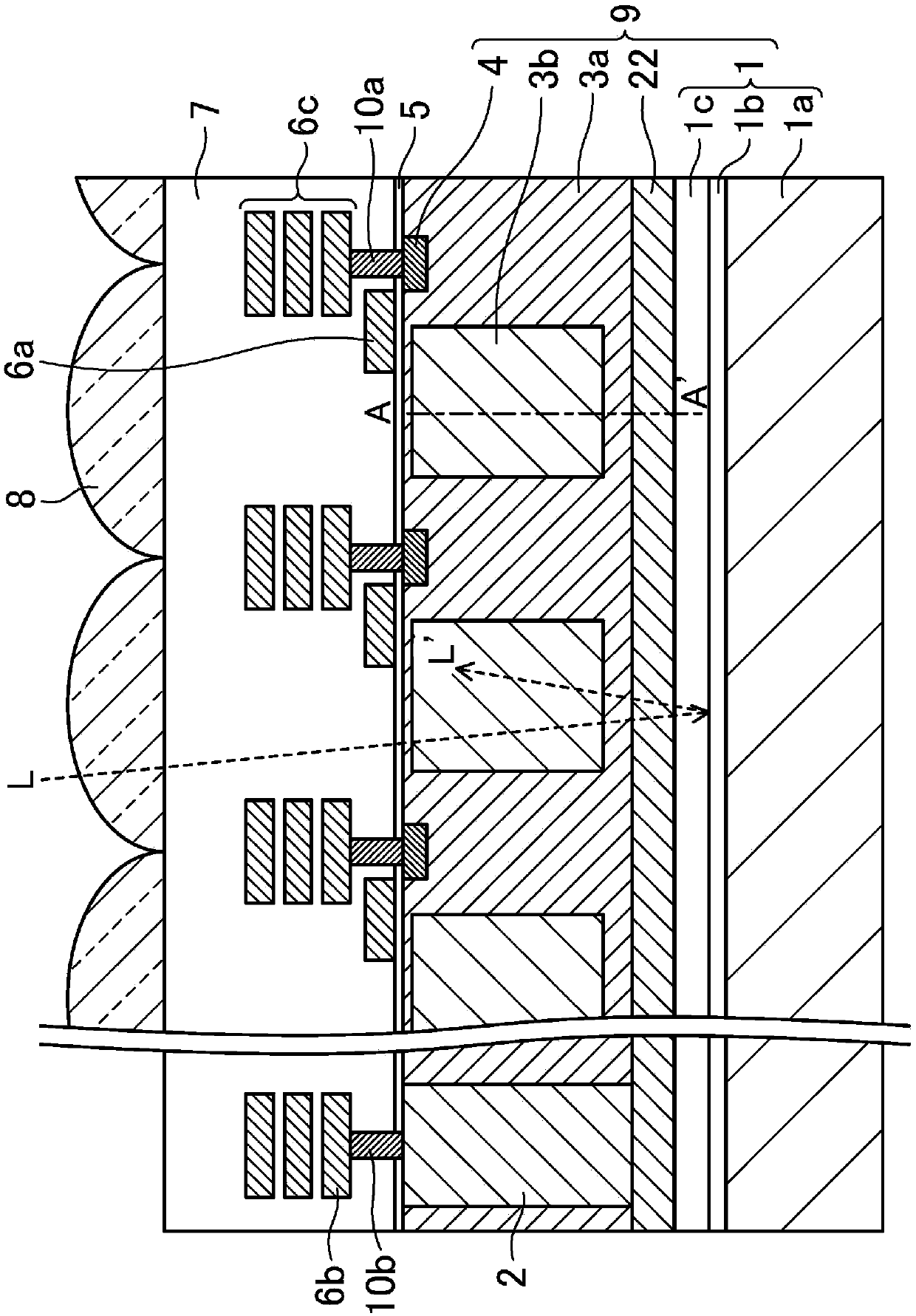
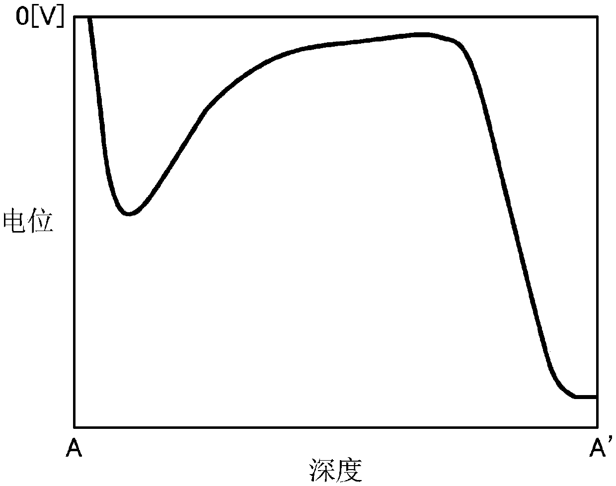
[0025] figure 1 It is a cross-sectional view of the solid-state imaging device according to the first embodiment disclosed in this specification.
[0026] Such as figure 1 As shown, the solid-state imaging device of this embodiment has: a substrate 9, a plurality of pixels are arranged two-dimensionally on the upper surface side of the substrate 9; a first impurity region 3a of the first conductivity type is provided on the Inside the substrate 9; a light receiving portion (photodiode) 3b of the second conductivity type provided on each of the plurality of pixels and formed in the first impurity region 3a; an overflow drain region 22 of the second conductivity type , which is provided in the substrate 9 under the first impurity region 3a; and the second conductivity type second impurity region 2, which is connected to the overflow drain region 22 in the first impurity region 3a. In this embodiment, the above-mentioned first conductivity type is, for example, p-type, and the ...
no. 2 approach
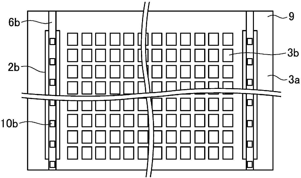
[0058] Figure 5 It is a cross-sectional view showing the solid-state imaging device according to the second embodiment disclosed in this specification. exist Figure 5 In , the same components as those of the solid-state imaging device according to the first embodiment are denoted by the same reference numerals.
[0059] Such as Figure 5 As shown, the solid-state image pickup device of this embodiment is a solid-state image pickup device that is irradiated with incident light from the back side of the substrate 29 . The solid-state image pickup device of this embodiment includes: a substrate 29; a first conductive type first impurity region 3a provided in the substrate 29; a second conductive type light receiving portion 3b provided in a plurality of pixels. each pixel, and formed in the first impurity region 3a; the overflow drain region 22 of the second conductivity type, which is provided under the first impurity region 3a in the substrate 29; and the second impurity r...
no. 3 approach
[0074] Figure 6A is a cross-sectional view showing an SOI substrate 50 having a gettering layer 41, Figure 6B It is a cross-sectional view showing the solid-state imaging device according to the third embodiment including the SOI substrate 50 .
[0075] Such as Figure 6A , Figure 6B As shown, the solid-state imaging device of the present embodiment is different from the solid-state imaging device of the first embodiment in that the gettering layer 41 is provided in the silicon layer 1 c of the SOI substrate 50 . The configurations of the insulating film 5 , the gate electrode 6 a , the wire 6 c , the planarizing film 7 , and the like are the same as those of the solid-state image pickup device according to the first embodiment.
[0076] It should be noted that, in Figure 6B Among them, substrate 49 has SOI substrate 50 , first impurity region 3 a , light receiving portion 3 b , drain region 4 and overflow drain region 22 . The configurations of the first impurity reg...
PUM
| Property | Measurement | Unit |
|---|---|---|
| thickness | aaaaa | aaaaa |
| thickness | aaaaa | aaaaa |
| refractive index | aaaaa | aaaaa |
Abstract
Description
Claims
Application Information
 - R&D
- Intellectual Property
- Life Sciences
- Materials
- Tech Scout
- Unparalleled Data Quality
- Higher Quality Content
- 60% Fewer Hallucinations
Browse by: Latest US Patents, China's latest patents, Technical Efficacy Thesaurus, Application Domain, Technology Topic, Popular Technical Reports.
© 2025 PatSnap. All rights reserved.Legal|Privacy policy|Modern Slavery Act Transparency Statement|Sitemap|About US| Contact US: help@patsnap.com