PCB production line

A PCB board and production line technology, applied in the field of digital direct writing exposure machine, can solve the problems of unstable quality, PCB board damage, hand fatigue, etc.

Pending Publication Date: 2019-04-05
源能智创(江苏)半导体有限公司
View PDF0 Cites 9 Cited by
  • Summary
  • Abstract
  • Description
  • Claims
  • Application Information

AI Technical Summary

Problems solved by technology

[0003] In the existing technology, there is no automatic production line to realize continuous operation between various processes, and manual intervention is required to operate in the middle. Stability, low efficiency and other issues, and it is easy to cause damage to the PCB board

Method used


Image

  • PCB production line
  • PCB production line
  • PCB production line

Examples


Embodiment Construction

[0027] The following will clearly and completely describe the technical solutions in the embodiments of the present invention with reference to the drawings in the embodiments of the present invention.

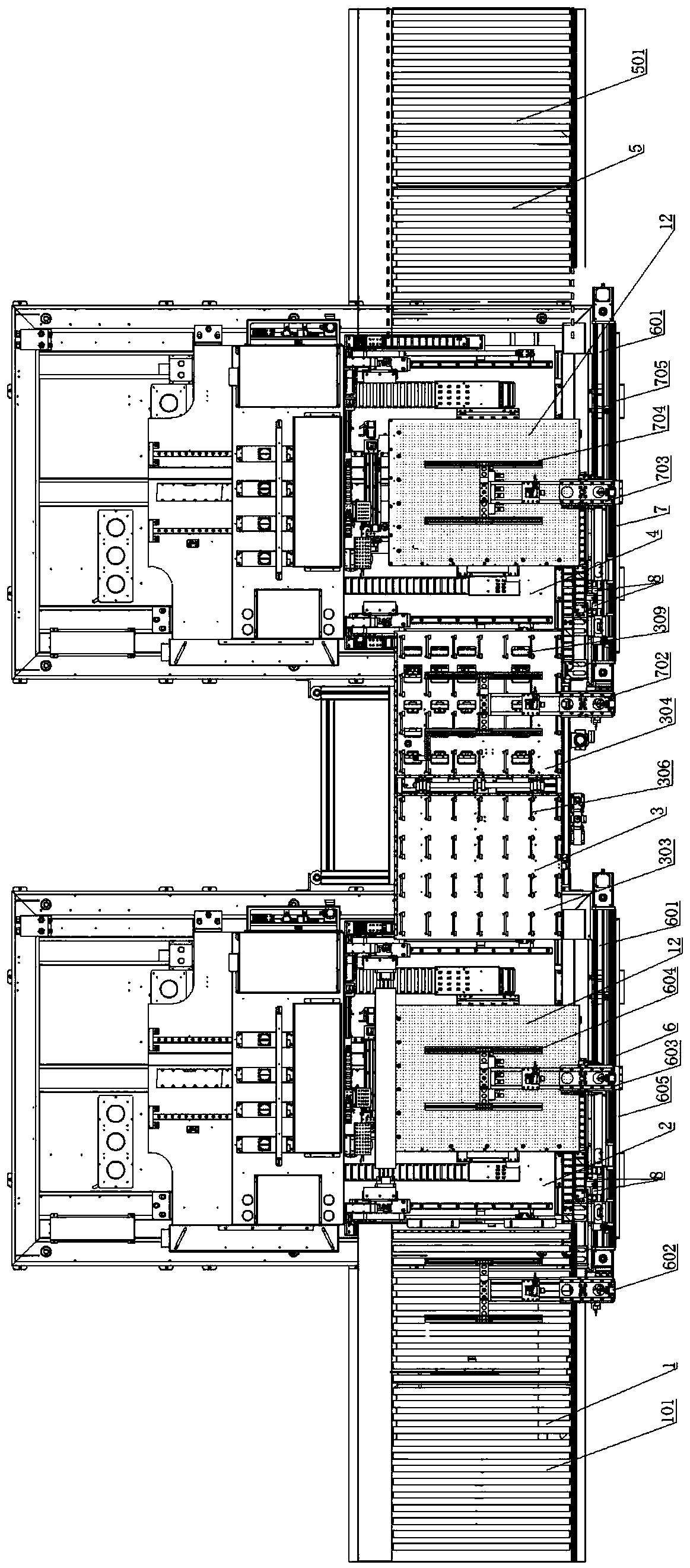
[0028] See figure 1 , a production line for PCB boards, including sequentially set:

[0029] The feeding conveyor 1 is used for feeding the PCB board, and the front side of the PCB board on the feeding conveyor 1 is facing upward and the back is facing downward;

[0030] The first photolithography machine 2 is used to expose and print patterns on the front side of the PCB board;

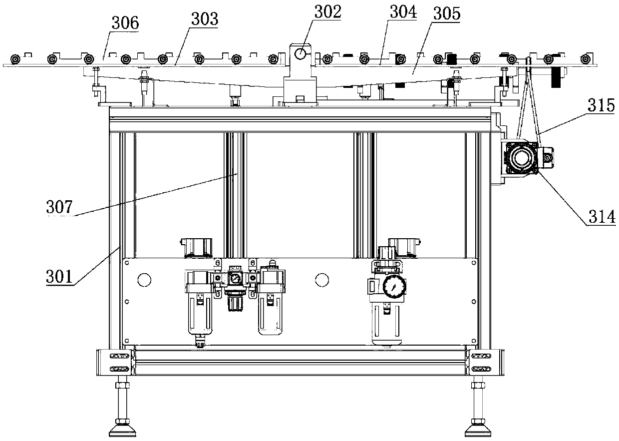
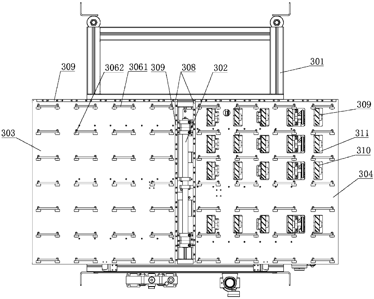
[0031] The board turning machine 3 is used to turn over the PCB board so that the back side of the PCB board faces up;

[0032] The second photolithography machine 4 is used to expose and print graphics on the back of the PCB board;

[0033] Discharging conveyor 5, used for the discharging of PCB board;

[0034] It also includes a first transfer machine 6 arranged on one side of the first photoli...


PUM


Abstract

The invention provides a PCB production line which can realize feeding, front face exposing, overturning, back face exposing and discharging of PCBs with high automation degree, improves the production efficiency and avoids damage to the PCBs at the same time. The PCB production line comprises the following components arranged in sequence: a feeding conveyor for feeding the PCBs; a first photoetching machine for exposing and printing patterns on the front faces of the PCBs; an overturning machine for overturning the PCBs; a second photoetching machine for exposing and printing patterns on theback sides of the PCBs; and a discharging conveyor for discharging the PCBs. The PCB production line further comprises a first loader and a second loader, wherein linear guide rails are arranged on the first loader and the second loader and provided with a forward moving manipulator arm and a backward moving manipulator arm, lifting mechanisms are separately arranged on the forward moving manipulator arm and the backward moving manipulator arm, and moving suckers are arranged on the lifting mechanisms.

Description

technical field [0001] The invention relates to the field of digital direct writing exposure machines, in particular to a production line of PCB boards. Background technique [0002] PCB (Printed Circuit Board), the Chinese name is printed circuit board, also known as printed circuit board, is an important electronic component, a support for electronic components, and a carrier for electrical connections of electronic components. Its development has a history of more than 100 years; its design is mainly layout design; the main advantage of using circuit boards is that it greatly reduces wiring and assembly errors, and improves automation and production labor rates. The PCB board needs to be processed on both sides during processing, which needs to realize the loading, front exposure, flipping, back exposure, and discharge of the PCB board. [0003] In the existing technology, there is no automatic production line to realize continuous operation between various processes, an...

Claims


Application Information

Patent Timeline
Patent Type & Authority Applications(China)
IPC IPC(8): H05K3/00B66F19/00B65G47/91
CPCH05K3/0008B65G47/912B66F19/00H05K2203/1545H05K2203/1563
Inventor 章卫平张雷李伟成
Owner 源能智创(江苏)半导体有限公司
Why Eureka
Try Eureka