Lateral diffused metal oxide semiconductor field effect transistor

A technology of oxide semiconductors and field effect transistors, which is applied in the field of laterally diffused metal oxide semiconductor field effect transistors, can solve problems such as burning integrated circuits, gate damage, and component damage, so as to reduce resistance, increase component area, and improve The effect of breakdown voltage and high temperature reverse bias test

Active Publication Date: 2019-04-09
NUVOTON
View PDF33 Cites 1 Cited by
  • Summary
  • Abstract
  • Description
  • Claims
  • Application Information

AI Technical Summary

Problems solved by technology

Electrostatic discharge currents, if not properly controlled, can burn integrated circuits and cause component damage
For example, if the electrostatic discharge current flows from the drain to the source of the device, it may also flow to the gate of the device, causing damage to the gate
[0004] In summary, although the existing LDMOS field effect transistors generally meet the needs, they are not satisfactory in all aspects, especially the electrostatic discharge current of LDMOS field effect transistors still needs to be further improved

Method used


Image

  • Lateral diffused metal oxide semiconductor field effect transistor
  • Lateral diffused metal oxide semiconductor field effect transistor
  • Lateral diffused metal oxide semiconductor field effect transistor

Examples


Embodiment Construction

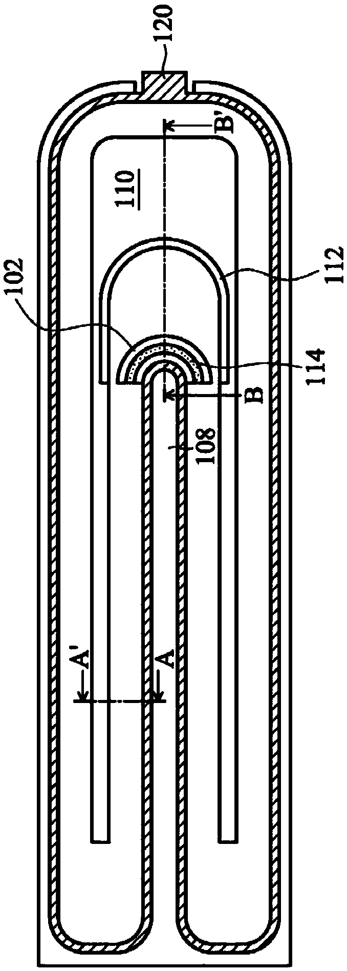
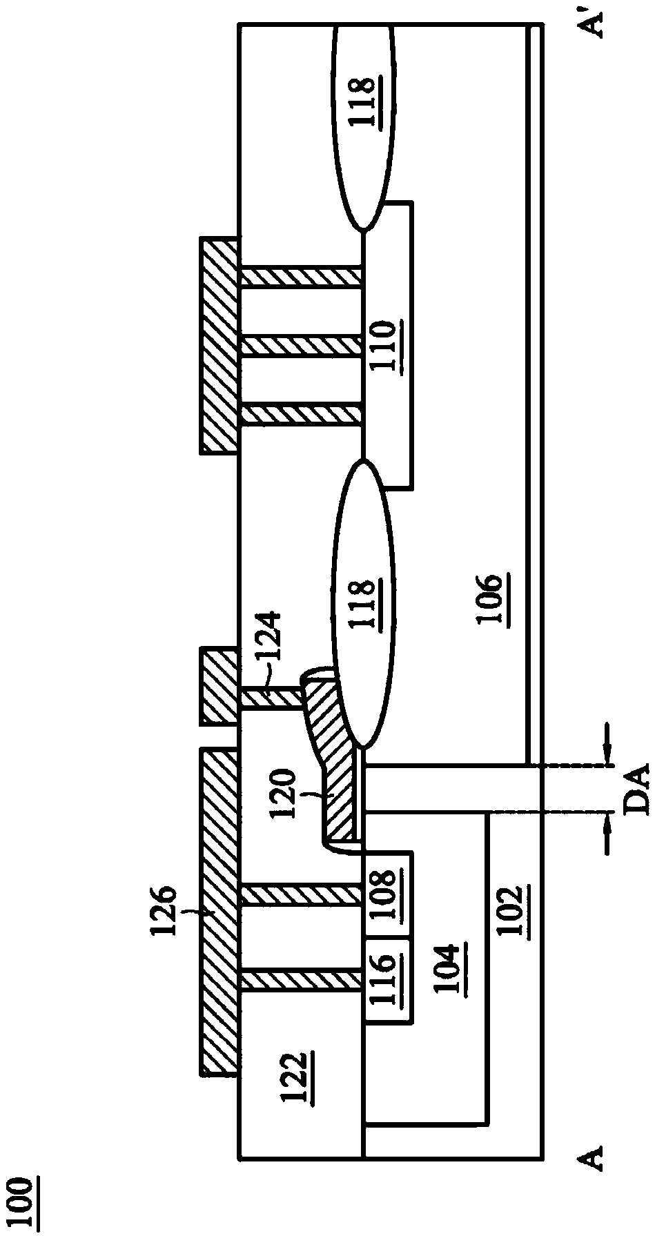
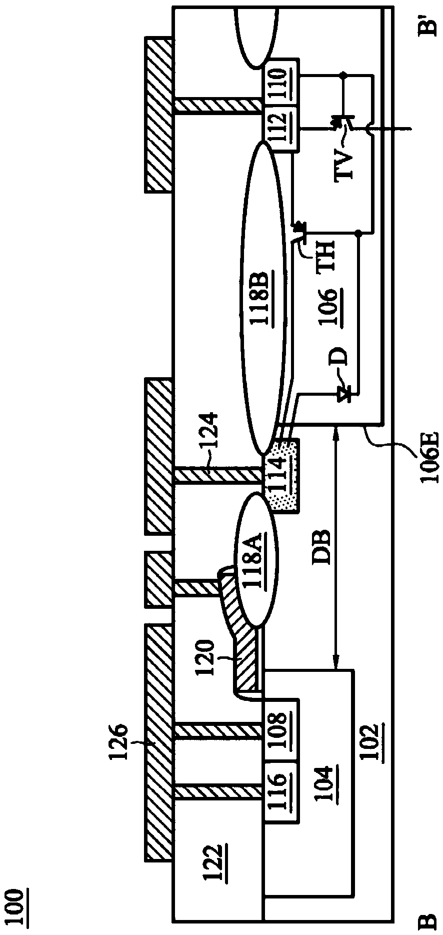
[0046] Many different implementation methods or examples are disclosed below to implement different features of the embodiments of the present invention, and specific elements and embodiments of their arrangement are described below to illustrate the embodiments of the present invention. Of course, these embodiments are only for illustration, and should not limit the scope of the embodiments of the present invention. For example, it is mentioned in the description that the first feature is formed on the second feature, which includes the embodiment that the first feature is in direct contact with the second feature, and also includes other features between the first feature and the second feature. Embodiments of the features, that is, the first feature is not in direct contact with the second feature. In addition, repeated symbols or signs may be used in different embodiments, and these repetitions are only for the purpose of simply and clearly describing the embodiments of th...


PUM


Abstract

Embodiments of the present invention provide a lateral diffused metal oxide semiconductor field effect transistor. The metal oxide semiconductor field effect transistor (MOSFET) comprises: a body region located on an upper portion of a substrate and having a first conductivity type; a drift region located at the upper part of the substrate and having a second conductivity type, wherein a first isolation region os arranged between the body region and the drift region; a grid positioned above the substrate; a source region located in the body region; a drain region in the drift region, comprising a first drain region and a second drain region disposed adjacent to each other, wherein the first drain region has a second conductivity type, and the second drain region having a first conductivitytype; a second isolation region disposed in a drift region between the first isolation region and the drain region; and a first doped region having a first conductivity type in the substrate betweenthe first isolation region and the second isolation region. The first doped region and the drift region form a first diode.

Description

technical field [0001] The embodiments of the present invention relate to a semiconductor technology, in particular to a laterally diffused metal oxide semiconductor field effect transistor. Background technique [0002] High-voltage semiconductor components are suitable for high-voltage and high-power integrated circuits. Conventional high voltage semiconductor devices include lateral diffused metal oxide semiconductor field effect transistors (lateral diffused metal oxide semiconductor, LDMOS). The advantage of high-voltage semiconductor components is that they are easily compatible with other processes and are cost-effective, so they are widely used in power supplies, power management, display driver IC components, communications, automotive electronics, industrial control and other fields. [0003] When the LDMOSFET is connected to an AC power source, a large amount of electrostatic charge may accumulate, and the electrostatic charge may flow at any two terminals to gen...

Claims


Application Information

Patent Timeline
Patent Type & Authority Applications(China)
IPC IPC(8): H01L29/78H01L29/06H01L27/02
CPCH01L27/0251H01L27/0255H01L27/0259H01L29/0615H01L29/0684H01L29/78
Inventor 韦维克陈柏安
Owner NUVOTON
Why Eureka
Try Eureka