Carrier plate and film coating equipment

A technology of coating equipment and carrier board, which is applied in the field of coating equipment, can solve the problems of silicon wafers being affected by air exposure, mechanical damage on the surface of silicon wafers, complicated and time-consuming problems, so as to avoid the influence of air exposure, reduce the probability of pollution, and improve work efficiency. efficiency effect

Pending Publication Date: 2019-04-16
鸿翌科技有限公司
View PDF5 Cites 4 Cited by
  • Summary
  • Abstract
  • Description
  • Claims
  • Application Information

AI Technical Summary

Problems solved by technology

[0003] It can be seen that in the existing double-sided solar cell manufacturing process, it is necessary to repeatedly break the vacuum in order to turn over the silicon wafer, so that the silicon wafer is frequently affected by air exposure during the entire manufacturing process; moreove

Method used


Image

  • Carrier plate and film coating equipment
  • Carrier plate and film coating equipment
  • Carrier plate and film coating equipment

Examples


Embodiment 1

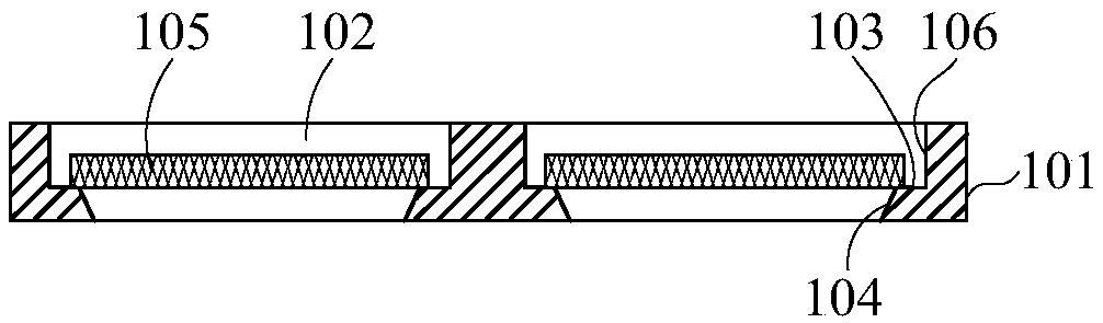
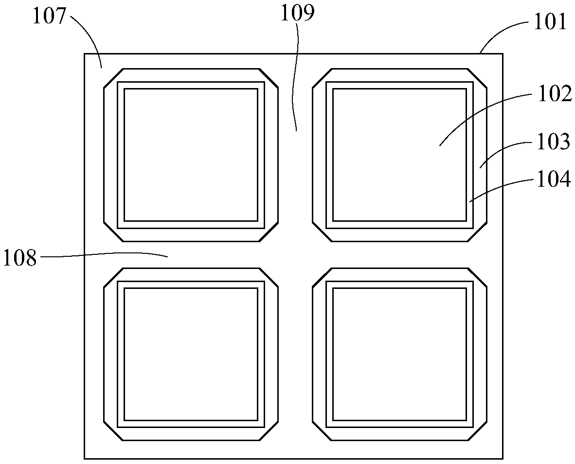
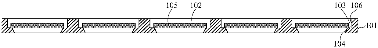
[0036] Such as Figure 1-Figure 4 As shown, the present embodiment provides a carrier 101 for carrying a silicon chip 105 (or other types of substrates), the carrier 101 is provided with at least one hollow groove 102, and each hollow groove 102 is provided with a support member So that the component to be processed (silicon wafer 105 ) can be placed in the hollow groove 102 .

[0037] Wherein, the size of the hollow groove 102 should match the size of the silicon wafer 105 placed therein. For example, most of the existing solar cells are octagonal, so the silicon wafers used to prepare the solar cells should also be octagonal. Correspondingly, the hollow groove can also be quadrangular or octagonal or other shapes, and the size of the hollow groove needs to be slightly larger than the silicon chip, so that the silicon chip can be put into it.

[0038] In this embodiment, after each silicon chip 105 (or other type of substrate) is placed in each hollow groove 102 on the carri...

Embodiment 2

[0066] Such as Figure 5-Figure 8 As shown, the present embodiment provides a coating device for coating a substrate (such as a silicon wafer), which includes: a coating chamber 200, and a driving device (not shown in the figure) arranged outside the coating chamber 200 , and the carrier plate 101 as described in Embodiment 1 disposed inside the coating chamber 200 .

[0067] Wherein, the interior of the coating chamber 200 is divided into a plurality of coating areas, and the top or bottom of each coating area is provided with a target installation position, and the corresponding target can be installed at the required position according to the needs of the coating, and the target is preferably a rolling target. . Each target can be controlled separately. Any two different targets can be made of the same material or different materials. For example, when the two targets are metal targets of different materials, an alloy film can be prepared. By modulating the magnetron The ...


PUM


Abstract

The invention provides a carrier plate and film coating equipment. The carrier plate is provided with at least one hollow groove, and each hollow groove is internally provided with a supporting component so that a part to be machined can be placed in the hollow groove. When the carrier plate and the film coating equipment are applied, in the film coating process, silicon wafer turning is not needed, therefore, repeated vacuum breaking is not needed, silicon wafers are prevented from being affected by air exposure in the film coating process, the probability that the silicon wafers are pollutedis reduced, the problems that working procedures for preparing two-face solar cell pieces in the prior art are tedious, therefore, the cell piece preparation efficiency is low, and the electric performance is poor are solved, the film layer quality of the cell pieces can be improved, the cell piece preparation time can be shortened, and therefore working efficiency is improved.

Description

technical field [0001] The present disclosure relates to the technical field of coating technology, in particular to a carrier plate used for coating processing and a coating device. Background technique [0002] Limited by the structure of the existing coating carrier, the coating process used by the coating equipment to produce double-sided solar cells is a single-side coating process. Specifically, the coating equipment includes a plurality of chambers, wherein a corresponding target is provided on the top of each chamber, adjacent chambers are separated by vacuum doors, and an automatic film turning machine is provided outside the chambers. After the silicon wafer is coated with the corresponding film layer in a chamber, the vacuum door needs to be opened to break the vacuum, and then the silicon wafer is turned over by the automatic flipper and placed in the next adjacent chamber, and then the adjacent next chamber The chamber is evacuated, and the corresponding film l...

Claims


Application Information

Patent Timeline
IPC IPC(8): C23C14/50C23C14/56
CPCC23C14/50C23C14/56
Inventor 沈良
Owner 鸿翌科技有限公司
Why Eureka
Try Eureka