Check patentability & draft patents in minutes with Patsnap Eureka AI!

Light-emitting diode pixel circuit and display panel

A technology of light-emitting diodes and pixel circuits, applied in static indicators, instruments, etc., can solve the problems of limited resolution of source chips, difficulty in accurately controlling LED current, etc., and achieve the effect of simple structure

Active Publication Date: 2019-04-16
SHENZHEN CHINA STAR OPTOELECTRONICS SEMICON DISPLAY TECH CO LTD
View PDF9 Cites 7 Cited by
  • Summary
  • Abstract
  • Description
  • Claims
  • Application Information

AI Technical Summary

Problems solved by technology

Because the resolution of the output voltage of the source chip is limited, it is difficult to precisely control the LED current to produce enough gray scales

Method used


Image

  • Light-emitting diode pixel circuit and display panel
  • Light-emitting diode pixel circuit and display panel
  • Light-emitting diode pixel circuit and display panel

Examples


Embodiment Construction

[0031] The present invention is particularly suitable for micro-light-emitting diode display panels, but is not limited to this, and can be applied to various current-driven display panels, such as organic light-emitting diode display panels and Mini LED display panels, which can improve driving current control accuracy.

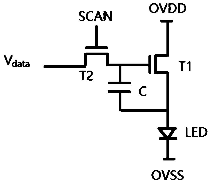
[0032] The present invention provides a pixel circuit that improves the original pixel circuit. The improved pixel circuit adds a capacitor and a thin film transistor on the basis of the original pixel circuit, and the increased capacitor is connected in series with the storage capacitor in the original pixel circuit. The added thin film transistor is connected to the common point of the two capacitors connected in series and the source of the driving thin film transistor (N-type).

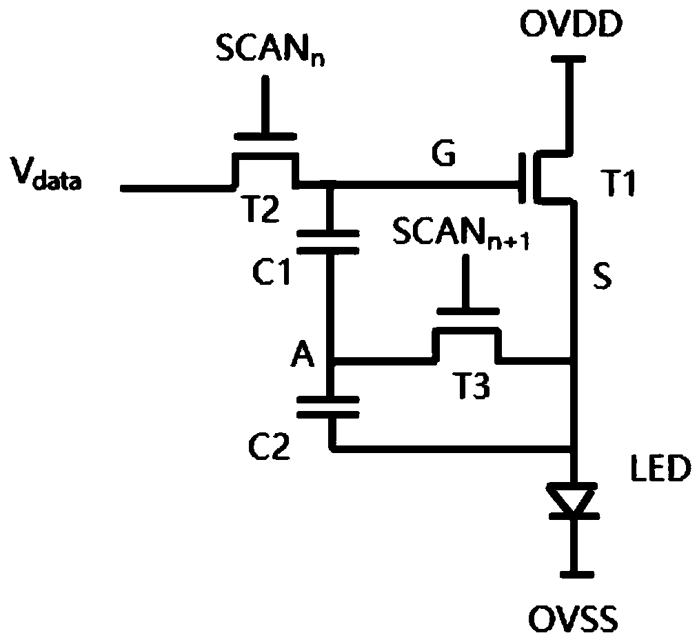
[0033] See image 3 and Figure 4 , image 3 Is a schematic circuit diagram of a preferred embodiment of a light-emitting diode pixel circuit of the present invention, Figure 4 for ...


PUM


Abstract

The invention relates to a light-emitting diode pixel circuit and a display panel. The light-emitting diode pixel circuit comprises a first thin film transistor (T1), a second thin film transistor (T2), a light-emitting diode (LED), a first capacitor (C1), a second capacitor (C2), and a third thin film transistor (T3), wherein the first thin film transistor (T1) is taken as a driving thin film transistor; a grid electrode of the first thin film transistor is connected with a first node (G); a source electrode and a drain electrode of the first thin film transistor are connected with a second node (S) and a power supply high voltage (OVDD); the second thin film transistor (T2) is taken as a switching thin film transistor; a grid electrode of the second thin film transistor is connected witha scanning signal (SCANn) of the row of pixels; a source electrode and a drain electrode of the second thin film transistor are connected with a first node (G) and a data signal (Vdata) respectively;a positive electrode of the light-emitting diode (LED) is connected with a second node (S); and a negative electrode of the light-emitting diode is connected with a power supply low voltage (OVSS). The invention also provides a corresponding display panel. According to the light-emitting diode pixel circuit and the display panel, the pixel circuit is improved in order that a source electrode chipwith relatively low output voltage resolution can be adopted for performing fine current control. The improved pixel circuit is simple in structure, and has no need of adding a driving signal.

Description

Technical field [0001] The present invention relates to the field of display technology, in particular to a light-emitting diode pixel circuit and a display panel. Background technique [0002] Organic light-emitting diode (OLED) display devices have many advantages such as self-luminescence, low driving voltage, high luminous efficiency, short response time, and wide operating temperature range, and are recognized by the industry as the display device with the most development potential. [0003] OLED display panels can be divided into passive matrix OLED (Passive Matrix OLED, PMOLED) and active matrix OLED (Active Matrix OLED, AMOLED) according to driving methods. Among them, the AMOLED panel has pixels arranged in an array, which is an active display type with high luminous efficiency, and is generally used in high-definition large-size display devices. [0004] Micro LED (Micro LED) display panel is a display device that uses high-density and small-size light-emitting diode (LED...

Claims


Application Information

Patent Timeline
Patent Type & Authority Applications(China)
IPC IPC(8): G09G3/3233
CPCG09G3/3233
Inventor 付舰航
Owner SHENZHEN CHINA STAR OPTOELECTRONICS SEMICON DISPLAY TECH CO LTD
Features
  • R&D
  • Intellectual Property
  • Life Sciences
  • Materials
  • Tech Scout
  • Unparalleled Data Quality
  • Higher Quality Content
  • 60% Fewer Hallucinations
Learn More