
Substrate embedded power device packaging structure and manufacturing method thereof

A power device and packaging structure technology, which is applied to the substrate-embedded power device packaging structure and its manufacturing field, can solve the problems of high cost, inability to metallize a single bare chip, complex process, etc.

Inactive Publication Date: 2019-05-07
NAT CENT FOR ADVANCED PACKAGING
View PDF5 Cites 24 Cited by
  • Summary
  • Abstract
  • Description
  • Claims
  • Application Information

AI Technical Summary

Problems solved by technology

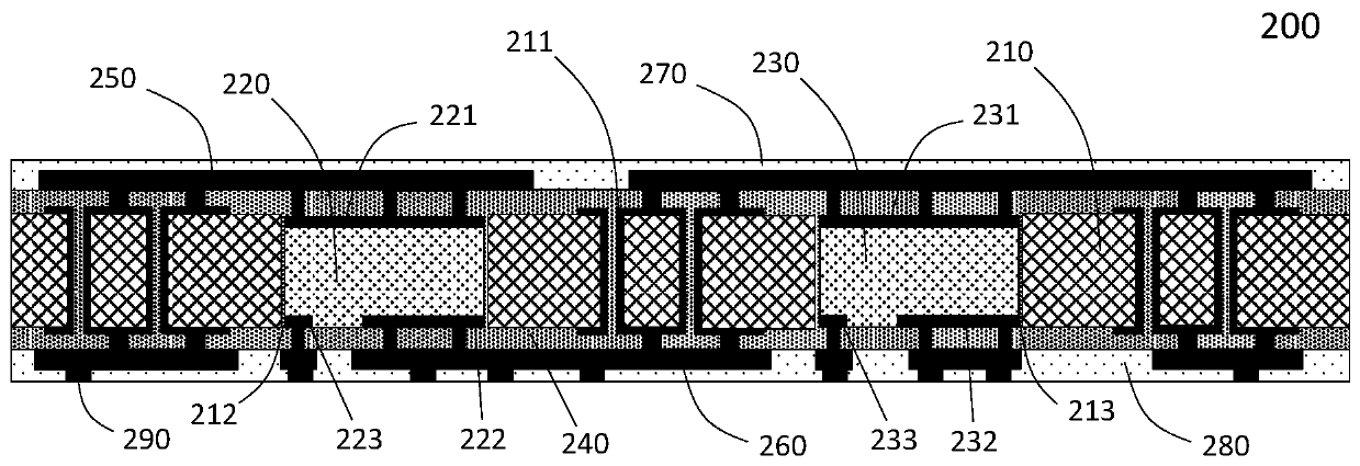
[0006] Aiming at the problems that the parasitic inductance of the existing power device aluminum wire bonding package may cause voltage overshoot, the heat dissipation effect is poor, the metallization of a single bare chip cannot be performed, the process is complicated, and the cost is relatively good, according to the present invention In one aspect, a substrate-embedded power device packaging structure is provided, including:

Method used


Image

  • Substrate embedded power device packaging structure and manufacturing method thereof
  • Substrate embedded power device packaging structure and manufacturing method thereof
  • Substrate embedded power device packaging structure and manufacturing method thereof

Examples


Embodiment Construction

[0039] In the following description, the present invention is described with reference to various examples. One skilled in the art will recognize, however, that the various embodiments may be practiced without one or more of the specific details, or with other alternative and / or additional methods, materials, or components. In other instances, well-known structures, materials, or operations are not shown or described in detail so as not to obscure aspects of the various embodiments of the invention. Similarly, for purposes of explanation, specific quantities, materials and configurations are set forth in order to provide a thorough understanding of embodiments of the invention. However, the invention may be practiced without these specific details. Furthermore, it should be understood that the various embodiments shown in the drawings are illustrative representations and are not necessarily drawn to scale.

[0040] In this specification, reference to "one embodiment" or "the...


PUM


Abstract

The invention discloses a substrate embedded power device packaging structure comprising: a substrate having a metalized through hole and a first power chip embedding slot; a first power chip disposedin the first power chip embedding slot; a photo-imageable dielectric (PID) covering the upper and lower sides of the substrate, and provided with an upper opening and a lower opening at positions corresponding to the metalized through hole and the electrode of the first power chip; an upper metal layer disposed on the upper surface of the PID and in the upper opening, and in electric interconnection to the first surface electrode of the first power chip and the metalized through hole; a lower metal layer disposed on the lower surface of the PID and in the lower opening, and in electric interconnection to the second surface electrode of the first power chip and the metalized through hole; an upper solder resist layer covering the upper metal layer; a lower solder resist layer covering thelower metal layer; and a metalized bonding pad.

Description

technical field [0001] The invention relates to the technical field of power device packaging, in particular to a substrate-embedded power device packaging structure and a manufacturing method thereof. Background technique [0002] The traditional aluminum wire-bonding package is the most commonly used and most mature packaging technology for power devices. Its package structure is as follows: figure 1 shown. However, there are several technical bottlenecks in aluminum wire-bonded packaging that restrict the performance improvement of power devices. The main problems are: most of the packaging materials used in aluminum wire-bonded packaging of power devices, such as tin-based lead-free solder, plastic packaging materials, etc., cannot withstand a high temperature environment above 200 degrees Celsius for a long time; gold-based solder is expensive; Lead solders are banned; high-melting-point solders require higher process temperatures, which consume energy and lead to hig...

Claims


Application Information

Patent Timeline
IPC IPC(8): H01L25/18H01L23/48H01L21/60
CPCH01L2224/18H01L2224/32225H01L2224/48227H01L2224/48472H01L2224/73265H01L2224/04105H01L2224/2518H01L2224/06181H01L2224/0603H01L2224/48091H01L2224/92144H01L2924/00012H01L2924/00014
Inventor 侯峰泽
Owner NAT CENT FOR ADVANCED PACKAGING
Learn More