Organic LED display substrate and manufacture method, and display device

A technology of light-emitting diodes and display substrates, applied in static indicators, semiconductor/solid-state device manufacturing, instruments, etc., can solve problems such as gate voltage changes, pixel gray scale abnormalities, changes, etc., to reduce parasitic capacitance and reduce voltage changes, voltage changes reduce the effect of

Active Publication Date: 2019-05-10
BOE TECH GRP CO LTD
View PDF3 Cites 8 Cited by
  • Summary
  • Abstract
  • Description
  • Claims
  • Application Information

AI Technical Summary

Problems solved by technology

[0004] When the grayscale of the pixel changes, the voltage on the data line will change, and a parasitic capacitance will be formed between the capacitor plate integrated with the gate of the driving TFT and the data line. When the voltage on the line changes, it will cause the voltage of the capacitor plate to change, which will cause the gate voltage of the driving TFT to change, resulting in abnormal gray scale of the pixel, resulting in abnormal display screen

Method used


Image

  • Organic LED display substrate and manufacture method, and display device
  • Organic LED display substrate and manufacture method, and display device
  • Organic LED display substrate and manufacture method, and display device

Examples


Embodiment Construction

[0052] In order to make the object, technical solution and advantages of the present invention clearer, the implementation manner of the present invention will be further described in detail below in conjunction with the accompanying drawings.

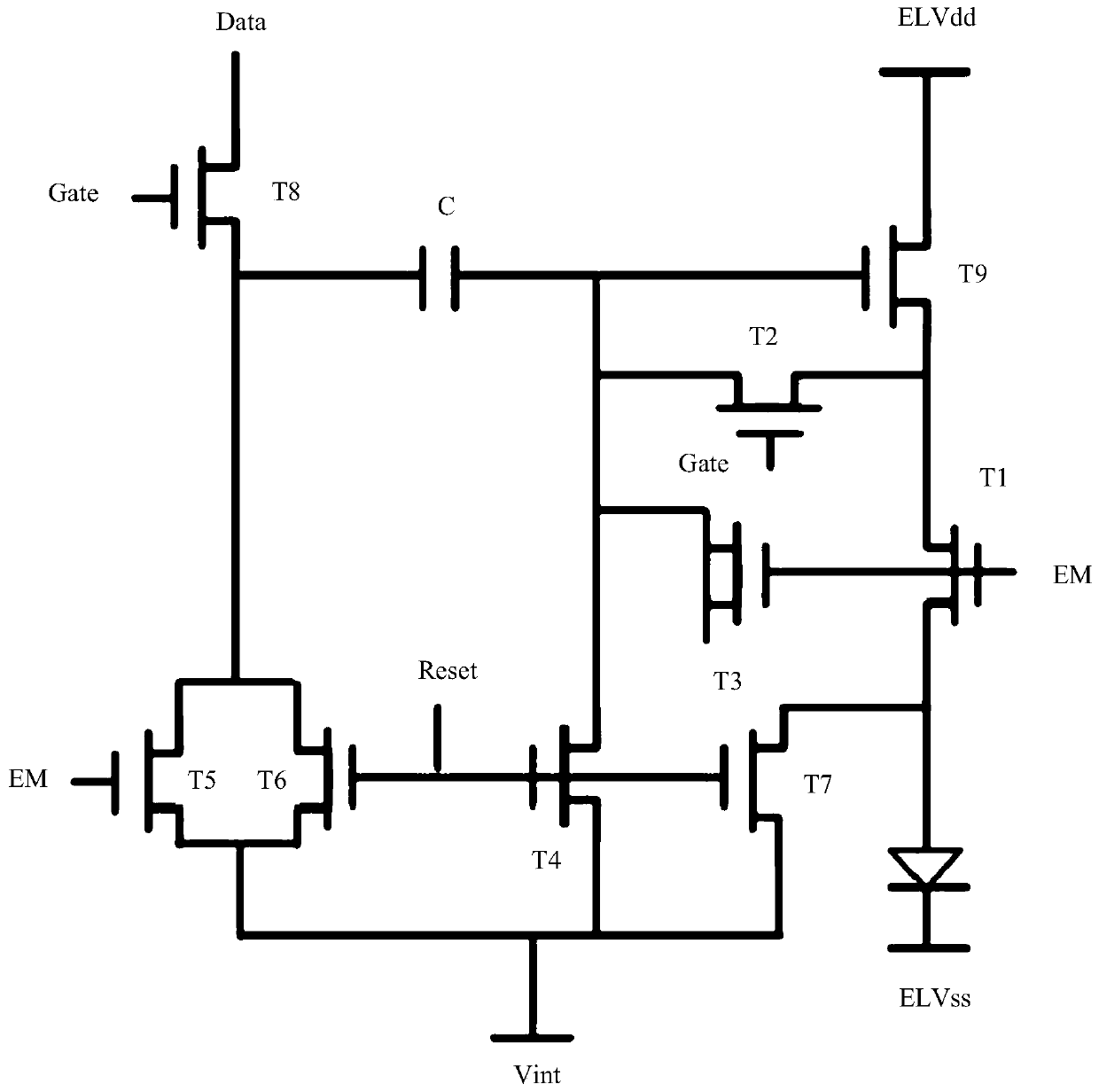
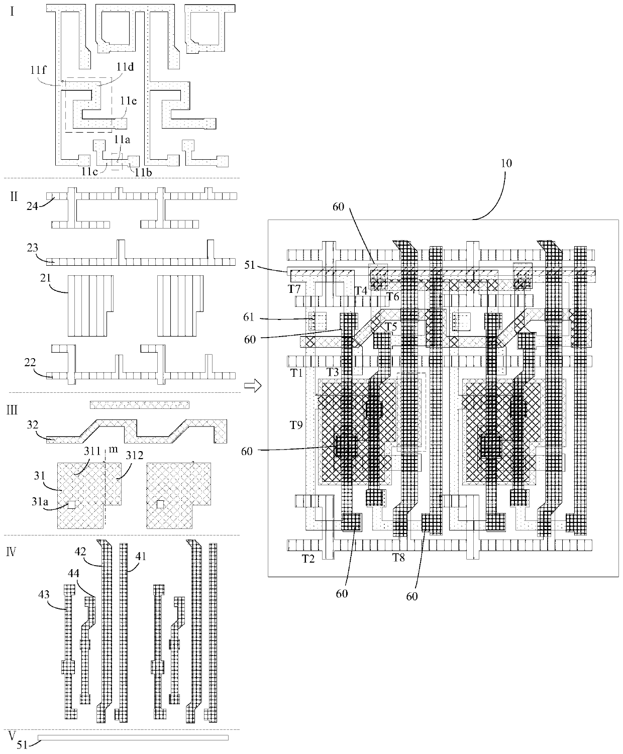
[0053] A schematic structural diagram of a display substrate provided by an embodiment of the present invention. The display substrate includes a base substrate, data lines, driving thin film transistors and energy storage capacitors located on the base substrate. The energy storage capacitor includes a first capacitor plate and a second capacitor plate, and the gate of the driving thin film transistor is integrally structured with the second capacitor plate. The first capacitive plate includes a body portion and a first shield portion. The main body is arranged opposite to the second capacitor plate, and the main body is located between the data line and the second capacitor plate in a direction perpendicular to the base substrate. ...


PUM


Abstract

The invention discloses an organic LED display substrate and a manufacture method, and a display device. The display substrate comprises a substrate, a data line, a drive film transistor, and an energy storage capacitor, wherein the energy storage capacitor comprises a first capacitance plate and a second capacitance plate, a gate of the drive film transistor and the second capacitance plate are integral, the first capacitance plate comprises a body part and a first shield part, the first shield part extends to the middle of the second capacitance plate and the data line adjacent to the secondcapacitance plate, the first shield part can shield capacitance coupling between the second capacitance plate and the data line adjacent to the second capacitance plate, so as to reduce parasitic capacitance between the second capacitance plate and the data line. When voltage of the data line changes, voltage generated by the second capacitance plate is lowered, lowering voltage of a control electrode of the film transistor, therefore, when gray level of the pixel changes, display image abnormality is relieved.

Description

technical field [0001] The invention relates to the field of display devices, in particular to an organic light emitting diode display substrate, a manufacturing method, and a display device. Background technique [0002] An organic light-emitting diode (Organic Light-Emitting Diode, OLED) display is a mainstream display that is widely used, and has the advantages of being ultra-thin and light, and low manufacturing cost. [0003] A display panel of an OLED display generally includes an array substrate and a cover plate oppositely arranged, and a light-emitting unit is arranged on the array substrate. The array substrate includes a base substrate and a plurality of data lines and a plurality of scan lines arranged on the base substrate. The plurality of data lines and the plurality of scan lines intersect each other to define a plurality of pixel regions. Each pixel area is provided with at least one driving TFT (Thin Film Transistor, thin film transistor), a switching TFT ...

Claims


Application Information

Patent Timeline
Patent Type & Authority Applications(China)
IPC IPC(8): H01L27/12H01L27/32H01L23/552H01L21/77
CPCG09G3/3233G09G2300/0819G09G2300/0861G09G2300/0852H10K59/1213H10K59/1216H10K59/126G09G3/3291
Inventor 陈义鹏王丽皇甫鲁江
Owner BOE TECH GRP CO LTD
Why Eureka
Try Eureka