GaN-based HEMT device and preparation method thereof

A device and cap layer technology, applied in the field of GaN-based HEMT devices and its preparation, can solve the problems of complex field plate design, increased gate leakage current, large dynamic on-resistance, etc., and achieve the effect of reducing the effect of current collapse

Inactive Publication Date: 2019-05-10
PEKING UNIV SHENZHEN GRADUATE SCHOOL
View PDF6 Cites 6 Cited by
  • Summary
  • Abstract
  • Description
  • Claims
  • Application Information

AI Technical Summary

Problems solved by technology

The ohmic contact on the p-GaN layer is easy to increase the leakage current of the gate
The P-GaN gate has a large d

Method used


Image

  • GaN-based HEMT device and preparation method thereof
  • GaN-based HEMT device and preparation method thereof
  • GaN-based HEMT device and preparation method thereof

Examples


Embodiment 1

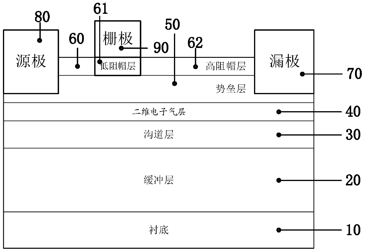
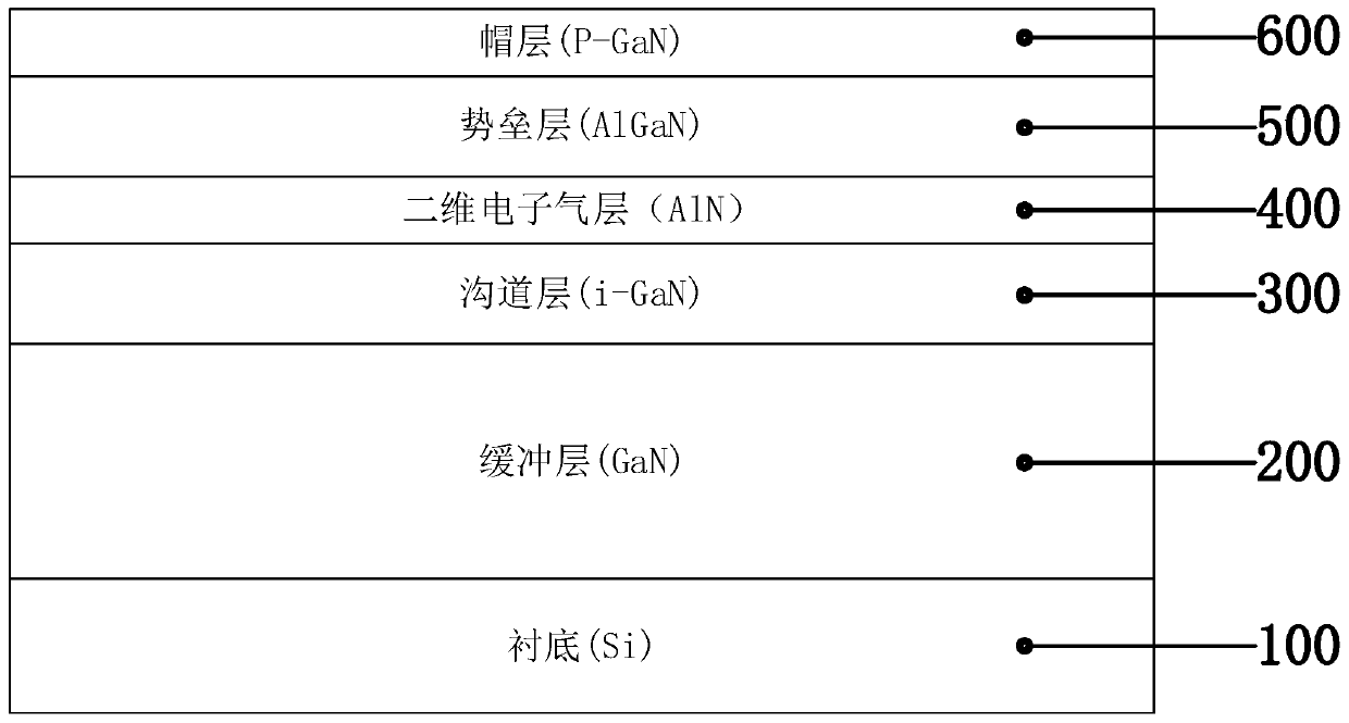
[0049] Such as figure 1 As shown, it is a schematic structural diagram of a GaN-based HEMT device in an embodiment. The GaN-based HEMT device disclosed in the present application includes a substrate 10, a buffer layer 20, a channel layer 30, a barrier layer 50, a cap layer 60, a source pole 80, gate 90 and drain 70. The buffer layer 20 is stacked on the substrate 10, the channel layer 30 is stacked on the buffer layer 20, the barrier layer 50 is stacked on the channel layer 30, and the cap layer 60 is stacked on the barrier layer 50 , the source 80 penetrates the cap layer 60 , the bottom of the source 80 is located on the barrier layer 50 , the drain 70 penetrates the cap layer 60 , and the bottom of the drain 70 is located on the barrier layer 50 . The gate 90 is located on the cap layer 60 . The drain 70, the source 80 and the gate 90 are not in contact with each other. The GaN-based HEMT device further includes a two-dimensional electron gas layer 40 , which is formed ...


PUM

PropertyMeasurementUnit
Thicknessaaaaaaaaaa
Thicknessaaaaaaaaaa
Thicknessaaaaaaaaaa

Abstract

The invention discloses a GaN-based HEMT device and a preparation method thereof. The GaN-based HEMT device comprises a substrate, a buffering layer, a channel layer, a potential barrier layer, a caplayer, a source electrode, a grid electrode and a drain electrode. Due to the fact that an H plasma processing technology is applied to prepare the cap layer to a high-impedance state to optimize theinternal electric field distribution of the GaN-base HEMT device in the preparation process of the GaN-base HEMT device, the influence of surface traps on the property of the device is reduced.

Description

technical field [0001] The invention relates to the field of semiconductor device manufacturing, in particular to a GaN-based HEMT device and a preparation method thereof. Background technique [0002] Power devices featuring low power consumption and high speed have recently attracted a lot of attention as the need for efficient and complete power conversion circuits and systems has increased. Wide bandgap semiconductor gallium nitride GaN material has the characteristics of large bandgap width, high critical breakdown electric field, and high electron saturation velocity, and has become an ideal material for a new generation of semiconductor power devices. In recent years, GaN-based HEMT devices represented by Al(ln, Ga, Sc)N / GaN can improve the safety of circuit operation. GaN-based HEMT devices are normally-on devices. In circuits, power elements of the normally-off type, also known as enhancement-mode (e-mode) transistors, are preferred for fail-safe operation. To re...

Claims


Application Information

Patent Timeline
IPC IPC(8): H01L29/778H01L29/207H01L29/06H01L21/265H01L21/335
Inventor 林信南石黎梦
Owner PEKING UNIV SHENZHEN GRADUATE SCHOOL
Why Eureka
Try Eureka