A gallium nitride based field effect transistor and its preparation method

A GaN-based field and transistor technology, applied in semiconductor/solid-state device manufacturing, semiconductor devices, electrical components, etc., can solve problems such as poor Schottky contact, insufficient component stability, and poor thermal stability. Achieve good thermal conductivity and thermal stability, reduce spontaneous thermal effects, and reduce current collapse effects

Active Publication Date: 2017-12-05
XIAMEN SANAN INTEGRATED CIRCUIT
View PDF4 Cites 0 Cited by
  • Summary
  • Abstract
  • Description
  • Claims
  • Application Information

AI Technical Summary

Problems solved by technology

However, metals that are commonly used at present, such as tungsten (W), have good thermal stability, and their melting point can reach above 3400°C, but the work function is too low, resulting in poor Schottky contact.
As a commonly used metal, molybdenum (Mo) has a melting point above 2600°C, but its thermal stability is not good, so it is difficult to meet the demand.
[0004] In addition, gallium nitride transistors generally work in depletion mode. To achieve enhancement mode work, fluorine (F) plasma treatment, N 2 O plasma treatment, but the plasma damage caused by plasma treatment will cause insufficient stability of components
In addition, there is also a way to use Cascode, but the manufacturing process is complicated, the packaging is special, the process requirements are high, and the yield rate is low, so it is difficult to apply in practice

Method used


Image

  • A gallium nitride based field effect transistor and its preparation method
  • A gallium nitride based field effect transistor and its preparation method
  • A gallium nitride based field effect transistor and its preparation method

Examples


Embodiment 1

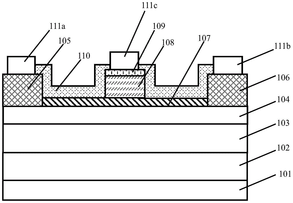
[0037] reference figure 1 In the transistor 100 of this embodiment, a substrate 101, a buffer layer 102, a gallium nitride layer 103, and an aluminum gallium nitride layer 104 are sequentially stacked from bottom to top. The upper surface of the aluminum gallium nitride layer 104 is provided with an active electrode 105, The drain 106 and the insulating layer 107 located therebetween, the insulating layer 107 is provided with a gate 108, and the top of the gate 108 is provided with a metal electrode layer 109. The above structure is covered with a passivation layer 110. The passivation layer 110 is provided with openings above the source electrode 105, the drain electrode 106 and the metal electrode layer 109, respectively, and thick electrodes 111a, 111b, and 111c are respectively provided in the openings .

[0038] The insulating layer 107 may be an oxide, such as Gd 2 O 3 , Pr 2 O 3 , La 2 O 3 , HfO 2 , ZrO 2 , Al 2 O 3 , Y 2 O 3 , Sc 2 O 3 , Er 2 O 3 , Ta 2 O 5 , HfZrO, AlLaO...

Embodiment 2

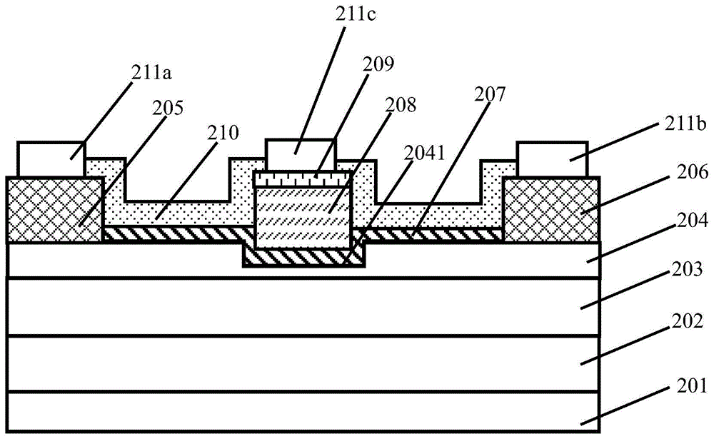
[0053] reference figure 2 In the transistor 200 of this embodiment, a substrate 201, a buffer layer 202, a gallium nitride layer 203, and an aluminum gallium nitride layer 204 are sequentially stacked from bottom to top. The upper surface of the aluminum gallium nitride layer 204 is provided with an active electrode 205 and The drain 206 and the insulating layer 207 between the two. A portion of the upper surface of the aluminum gallium nitride layer 204 is recessed to form a trench 2041, and the insulating layer 207 is also recessed accordingly. The insulating layer 107 is provided with a gate 208 made of conductive diamond-like carbon at a position corresponding to the trench 2041, and a metal electrode layer 209 is provided on the top of the gate 208. The above structure is covered with a passivation layer 210. The passivation layer 210 is provided with openings above the source electrode 205, the drain electrode 206, and the metal electrode layer 209, and thickened electro...

Embodiment 3

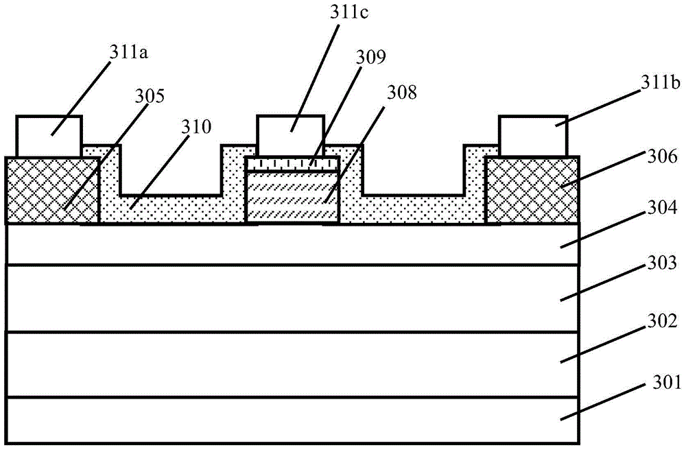
[0062] reference image 3 In the transistor 300 of this embodiment, a substrate 301, a buffer layer 302, a gallium nitride layer 303, and an aluminum gallium nitride layer 304 are sequentially stacked from bottom to top. The upper surface of the aluminum gallium nitride layer 304 is provided with an active electrode 305, The drain 306 and the gate 308 located between the two, the top of the gate 308 is provided with a metal electrode layer 309. The above structure is covered with a passivation layer 310. The passivation layer 310 is provided with openings above the source 305, drain 306, and metal electrode layer 309, and thickened electrodes 311a, 311b, and 311c are respectively provided in the openings .

[0063] The gate 308 is a p-type doped conductive DLC, and pure DLC is doped with less than 5wt% of boron (B), aluminum (Al), indium (In) or a combination thereof. The materials of the other components are the same as in Embodiment 1, and will not be repeated here. As the ga...


PUM


Abstract

The invention discloses a gallium nitride-based field effect transistor, comprising a substrate, a buffer layer, a gallium nitride (GaN) layer, an aluminum gallium nitride (AlGaN) layer sequentially stacked from bottom to top, and a A source electrode, a drain electrode and a gate electrode located therebetween on the aluminum gallium layer, the gate electrode is made of conductive diamond-like carbon (DLC), and in the conductive DLC, the sp2 bond is The content is greater than 50%. The invention uses diamond-like carbon as the gate material to reduce the spontaneous thermal effect of the gate region, improve the stability, and at the same time adjust the gate resistance and polarity by doping diamond-like carbon to achieve the purpose of enhanced operation. The invention also discloses a preparation method of the above transistor.

Description

Technical field [0001] The invention relates to a semiconductor device, in particular to a gallium nitride-based field effect transistor and a preparation method thereof. Background technique [0002] Gallium nitride (GaN) is a representative of the third generation of semiconductors. It has excellent electrical characteristics such as wide band gap, high breakdown field strength, and high saturated electron drift rate. It has gradually attracted attention in the field of semiconductor devices. Among them, GaN-based high electron migration High-speed transistor devices have become the first choice for high-frequency, high-voltage, high-temperature and high-power applications. The conventional GaN-based high electron mobility transistor uses a heterostructure of AlGaN / GaN to form a two-dimensional electron gas layer (2-DGE), and controls the two-dimensional electron by changing the gate voltage between the source and the drain. The electron concentration of the gas, thereby contr...

Claims


Application Information

Patent Timeline
Patent Type & Authority Patents(China)
IPC IPC(8): H01L29/778H01L29/43H01L29/06H01L21/337
Inventor 叶念慈徐宸科林科闯
Owner XIAMEN SANAN INTEGRATED CIRCUIT
Why Eureka
Try Eureka