
Field effect transistor

A technology of field-effect transistors and transistors, which is applied in the direction of semiconductor devices, semiconductor/solid-state device manufacturing, electrical components, etc., can solve the problems of current collapse, inability to effectively reduce, and inability to effectively passivate the surface of materials, so as to reduce electric field and reduce parasitic Capacitance, the effect of reducing the effect of current collapse

Active Publication Date: 2013-01-30
DYNAX SEMICON
View PDF0 Cites 0 Cited by
  • Summary
  • Abstract
  • Description
  • Claims
  • Application Information

AI Technical Summary

Problems solved by technology

[0007] Second, the current collapse effect caused by air ionization
However, SiO2, SiON and other dielectric layers have been studied and tried. Compared with SiN and GaN, they cannot effectively passivate the surface of the material, and cannot effectively reduce the damage caused by the surface state of GaN.

Method used


Image

  • Field effect transistor
  • Field effect transistor
  • Field effect transistor

Examples


Embodiment Construction

[0028] The preferred embodiments of the present invention will be described in detail below in conjunction with the accompanying drawings.

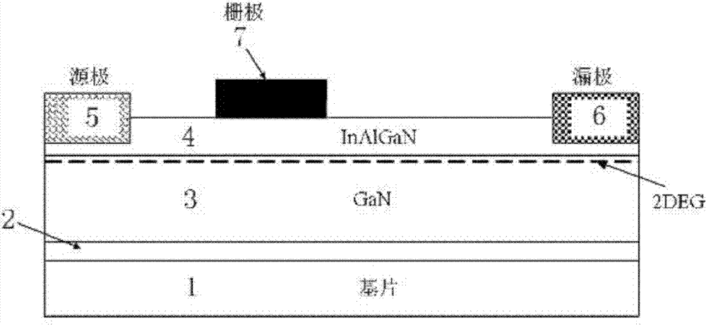
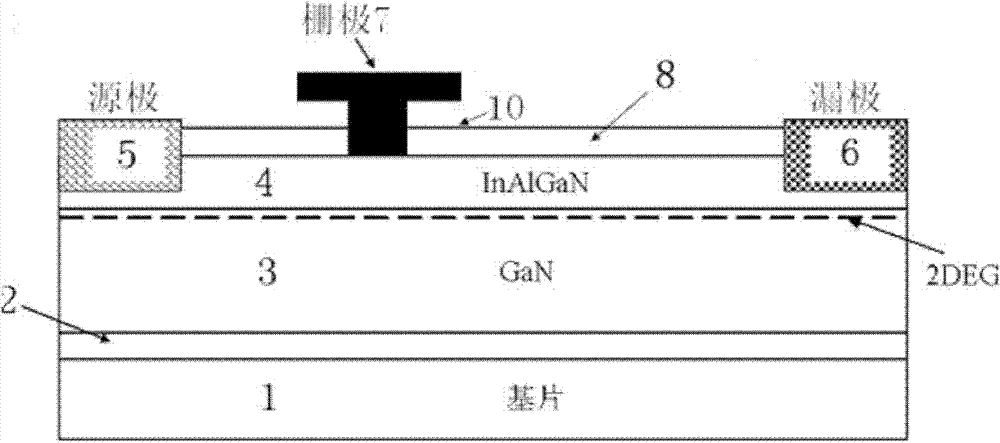
[0029] see Figure 4 As shown, the material of the substrate 1 can be sapphire (Sapphire), SiC, GaN, Si or any other material suitable for growing gallium nitride known to those skilled in the art. The deposition method of the substrate 1 includes CVD, VPE, MOCVD, LPCVD, PECVD, pulsed laser deposition (PLD), atomic layer epitaxy, MBE, sputtering, evaporation, etc.

[0030] On the substrate 1 is an optional nucleation layer 2 for growing a semiconductor layer thereon. In the present invention, the nucleation layer 2 may not be formed, but the semiconductor layer may be directly formed on the substrate 1 .

[0031] On the nucleation layer 2 is a semiconductor layer 3, which can be any semiconductor material based on nitride, such as a group III nitride semiconductor material, wherein the III valence atoms include indium, aluminum, gallium ...


PUM


Abstract

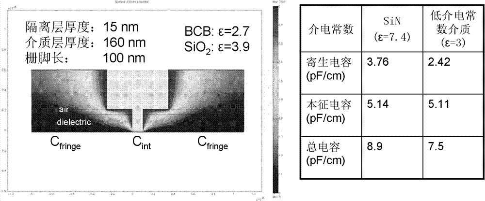
The invention provides a field effect transistor. The surface of the transistor is provided with a first dielectric layer and a second dielectric layer, wherein the second dielectric layer is arranged on the first dielectric layer; the dielectric constants of the materials of the first dielectric layer and the second dielectric layer are different; and the material of the second dielectric layer has low dielectric constant. In the field effect transistor of the invention, the second dielectric layer with low dielectric constant is arranged on the first dielectric layer; the first dielectric layer is used to passivate the defects and surface states of the material; the second dielectric layer is used to reduce the air ionization effect in a strong field; and the second dielectric layer with low dielectric constant can be used to greatly reduce the parasitic capacitance of elements and increase the cut-off frequency of elements. With the help of the first dielectric layer and the second dielectric layer, a field plate structure can be formed, and the field plate structure facilitates to further reduce the electrical field strength and the current collapse effect.

Description

technical field [0001] The invention relates to a field effect transistor. Background technique [0002] The dielectric breakdown electric field of the third-generation semiconductor gallium nitride (GaN) is much higher than that of the first-generation semiconductor silicon (Si) or the second-generation semiconductor gallium arsenide (GaAs), up to 3MV / cm, so that its electronic devices can withstand very high voltage. At the same time, gallium nitride can form a heterojunction structure with other gallium-based compound semiconductors (group III nitride semiconductors). Due to the strong spontaneous polarization and piezoelectric polarization effects of III-nitride semiconductors, a two-dimensional electron gas (2DEG) channel with a high electron concentration can be formed near the interface of the heterojunction. This heterojunction structure also effectively reduces the scattering of ionized impurities, so the electron mobility in the channel is greatly improved. Gall...

Claims


Application Information

Patent Timeline
Patent Type & Authority Patents(China)
IPC IPC(8): H01L29/778H01L29/06H01L21/335
Inventor 范爱民
Owner DYNAX SEMICON
Learn More