A transistor based on an enhanced gate structure and its preparation method

A gate structure, enhanced technology, applied in semiconductor/solid-state device manufacturing, semiconductor devices, electrical components, etc., can solve the problems of insufficient stability of components, complex manufacturing process, high process requirements, etc., to reduce spontaneous thermal effects, Simple process and strong controllability

Active Publication Date: 2018-08-24
XIAMEN SANAN INTEGRATED CIRCUIT
View PDF4 Cites 0 Cited by
  • Summary
  • Abstract
  • Description
  • Claims
  • Application Information

AI Technical Summary

Problems solved by technology

[0004] In addition, HEMTs generally work in depletion mode. To achieve enhanced work, fluorine (F) plasma treatment, N 2 O plasma treatment, but the plasma damage caused by plasma treatment will cause insufficient stability of the components; there is also a way to use Cascode, but the manufacturing process is complicated, the packaging is special, the process requirements are high, and the yield rate is low, so it is difficult to be practical application

Method used


Image

  • A transistor based on an enhanced gate structure and its preparation method
  • A transistor based on an enhanced gate structure and its preparation method
  • A transistor based on an enhanced gate structure and its preparation method

Examples


Embodiment 1

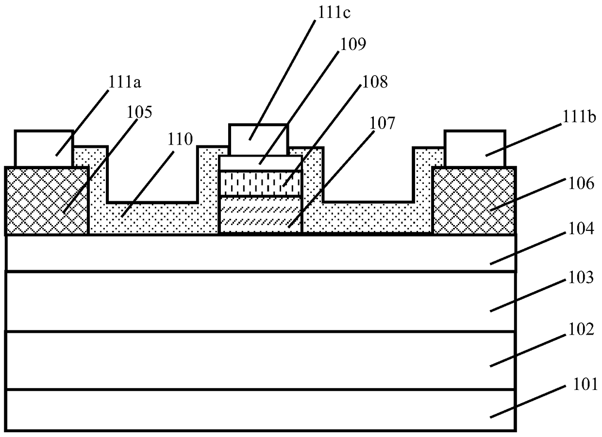
[0037] refer to figure 1 , the transistor 100 of this embodiment has a substrate 101, a buffer layer 102, a gallium nitride layer 103, and a barrier layer 104 stacked sequentially from bottom to top, and the upper surface of the barrier layer 104 is provided with a source 105, a drain 106, and The gate 107 located between the two has a DLC layer 108 and a metal electrode layer 109 stacked on top of the gate 107 in sequence. A passivation layer 110 is covered on the above structure, and the passivation layer 110 is respectively provided with openings above the source electrode 105, the drain electrode 106 and the metal electrode layer 109, and thickened electrodes 111a, 111b and 111c are respectively provided in the openings .

[0038] The barrier layer 104 is AlGaN; the gate 107 is p-type Al 1-x Ga x N, where 0≤x≤1. AlGaN and Al 1-x Ga x The p-n contact surface is formed between N, and its potential barrier is higher than that caused by ordinary Schottky contact (metal g...

Embodiment 2

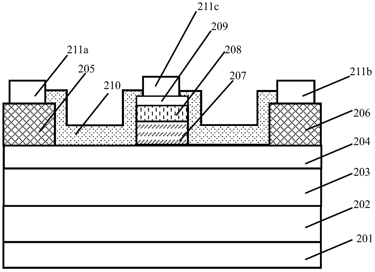
[0051] refer to figure 2 , the transistor 200 of this embodiment has a substrate 201, a buffer layer 202, a gallium nitride layer 203, and a barrier layer 204 stacked sequentially from bottom to top, and the upper surface of the barrier layer 204 is provided with a source 205, a drain 206, and The gate 207 located between the two has a DLC layer 208 and a metal electrode layer 209 stacked on top of the gate 207 in sequence. The passivation layer 210 is covered on the above structure, and the passivation layer 210 is respectively provided with openings above the source electrode 205, the drain electrode 206 and the metal electrode layer 209, and thickened electrodes 211a, 211b and 211c are respectively provided in the openings. .

[0052] The barrier layer 204 is InAlGaN; the gate 207 is p-type In 1-y-z Ga y Al z N, where 0≤y≤1; 0≤z≤1. InAlGaN and In 1-y-z Ga y Al z The p-n contact surface is formed between N, and its potential barrier is higher than that caused by ord...

Embodiment 3

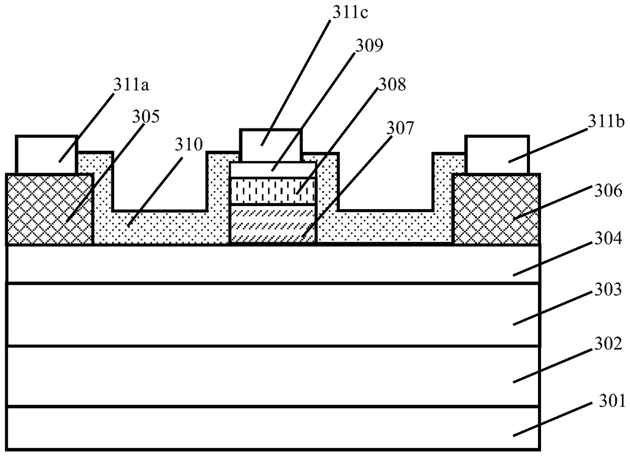
[0055] refer to image 3 , the transistor 300 of this embodiment has a substrate 301, a buffer layer 302, a gallium nitride layer 303 and a barrier layer 304 stacked in sequence from bottom to top, and a source 305, a drain 306 and a source 305 are arranged on the upper surface of the barrier layer 304. The gate 307 located between the two has a DLC layer 308 and a metal electrode layer 309 stacked on top of the gate 307 in sequence. A passivation layer 310 is covered on the above structure, and the passivation layer 310 is respectively provided with openings above the source electrode 305, the drain electrode 306 and the metal electrode layer 309, and thickened electrodes 311a, 311b and 311c are respectively provided in the openings. .

[0056] In this embodiment, the DLC layer 308 is p-type doped DLC, the content of sp2 bonds is greater than 50%, and doped with less than 5wt% of boron (B), aluminum (Al), indium (In) or a combination thereof. The materials of other compone...


PUM


Abstract

The invention discloses a transistor based on an enhanced grid structure. The transistor comprises a substrate, a buffer layer, a GaN (gallium nitride) layer, a barrier layer, a source electrode, a drain electrode and a grid electrode, wherein the substrate, the buffer layer, the GaN layer and the barrier layer are sequentially stacked from bottom to top, the source electrode is arranged on an aluminum gallium nitride layer, the grid electrode is positioned between the source electrode and the drain electrode, and the barrier layer is AlGaN or InAlGaN, and the grid electrode is p-type Al1-xGaxN (0<=x<=1) or p-type In1-y-zGayAlzN (0<=y<=1; 0<=z<=1). A DLC (Diamond-like carbon) layer is arranged on the grid electrode, and the content of sp2 keys of DLC is higher than 50%. According to the transistor, enhanced operation is realized, the self-heating effect of a transistor device can be reduced by diamond-like carbon, and stability is improved. The invention further provides a preparation method of the transistor.

Description

technical field [0001] The invention relates to a semiconductor device, in particular to a transistor based on an enhanced gate structure and a preparation method thereof. Background technique [0002] High Electron Mobility Transistor (HEMT) utilizes the two-dimensional electron gas layer (2-DGE) existing at the heterojunction interface, and controls the electron concentration of 2-DGE between the source and drain by changing the gate pressure, thereby Control work status. HEMTs are a new generation of transistors that are the first choice for high-frequency, high-voltage, high-temperature and high-power applications due to their excellent performance. [0003] In current HEMTs, common metal materials are mostly used as gate materials. Due to its high current and high voltage operation, the thermal stability and heat dissipation of gates have always been important research topics. However, metals that are commonly used at present, such as tungsten (W), have good thermal ...

Claims


Application Information

Patent Timeline
Patent Type & Authority Patents(China)
IPC IPC(8): H01L29/778H01L29/423H01L29/43H01L21/28H01L21/314H01L21/335
CPCH01L29/42316H01L29/432H01L29/66409H01L29/778
Inventor 叶念慈徐宸科林科闯
Owner XIAMEN SANAN INTEGRATED CIRCUIT
Why Eureka
Try Eureka