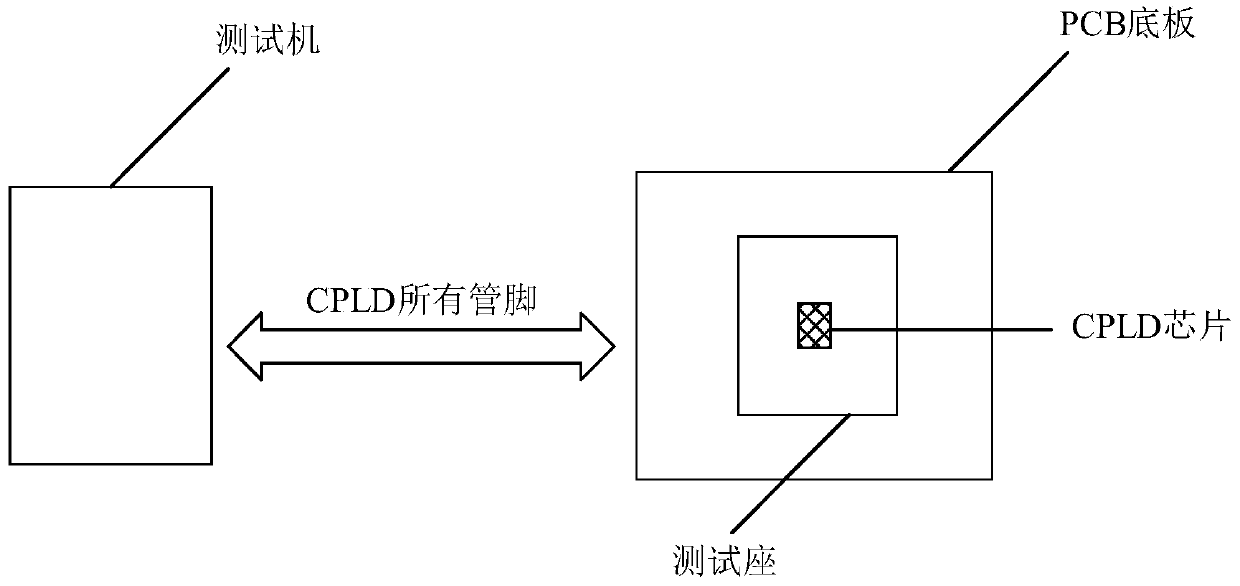
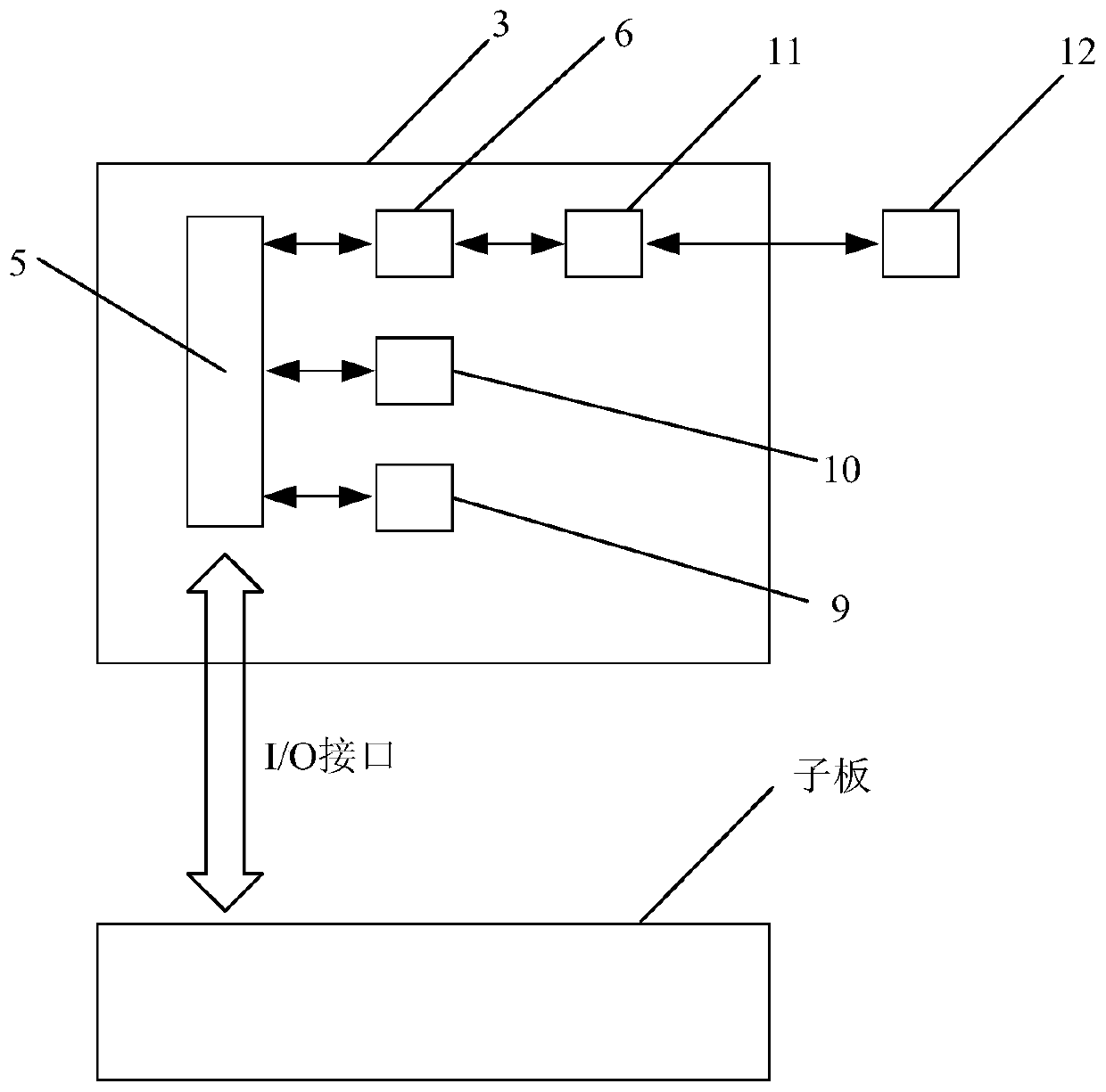
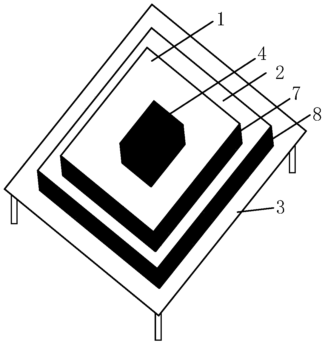
Test plate of CPLD chip based on FPGA/MCU
A test board and chip technology, applied in the field of integrated circuits, can solve the problems of long time period, high return test cost, unfavorable abnormal analysis, etc., and achieve the effect of good real-time performance, full performance test, and convenient after-sales maintenance.
- Summary
- Abstract
- Description
- Claims
- Application Information
AI Technical Summary
Problems solved by technology
Method used
Image

Examples
Embodiment Construction
[0024] The present invention will be described in further detail below in conjunction with specific examples, but the embodiments of the present invention are not limited thereto.
[0025] It should be noted that the terminology used here is only for describing specific implementations, and is not intended to limit the exemplary implementations according to the present application. As used herein, unless the context clearly indicates otherwise, the singular form is also intended to include the plural form. In addition, it should also be understood that when the terms "comprising" and / or "comprising" are used in this specification, it indicates There are features, steps, operations, means, components and / or combinations thereof. For the convenience of description, spatially relative terms may be used here, such as "on ...", "over ...", "on the surface of ...", "above", etc., to describe the The spatial positional relationship between one device or feature shown and other devic...
PUM
 Abstract
Description
Claims
Application Information
 - R&D
- Intellectual Property
- Life Sciences
- Materials
- Tech Scout
- Unparalleled Data Quality
- Higher Quality Content
- 60% Fewer Hallucinations
Browse by: Latest US Patents, China's latest patents, Technical Efficacy Thesaurus, Application Domain, Technology Topic, Popular Technical Reports.
© 2025 PatSnap. All rights reserved.Legal|Privacy policy|Modern Slavery Act Transparency Statement|Sitemap|About US| Contact US: help@patsnap.com