
Low temperature formation of high quality silicon oxide films in semiconductor device manufacturing

A semiconductor, silicon oxide layer technology, applied in semiconductor/solid state device manufacturing, electrical components, gaseous chemical plating, etc., can solve problems such as film cracking, reliability problems, affecting electrical and optical properties, etc.

Active Publication Date: 2019-05-21
LAM RES CORP
View PDF2 Cites 2 Cited by
  • Summary
  • Abstract
  • Description
  • Claims
  • Application Information

AI Technical Summary

Problems solved by technology

Compressive stress in the deposited film can cause the film to bubble or buckle, while tensile stress in the film can cause the film to crack
Additionally, wafer distortions caused by these stresses can lead to reliability issues in other device layers and often adversely affect electrical and optical performance, as well as the mechanical integrity of fabricated semiconductor devices

Method used

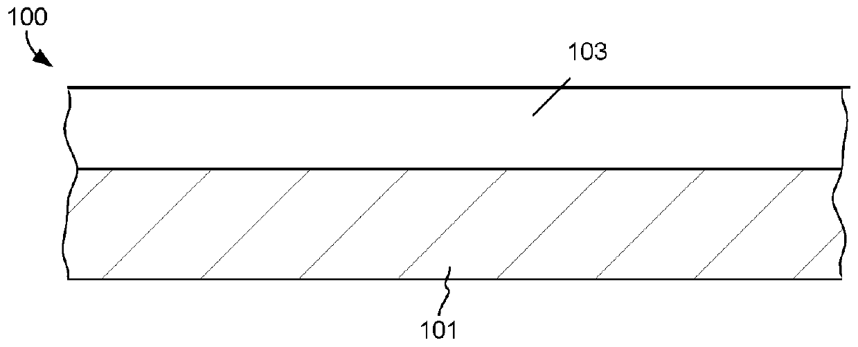
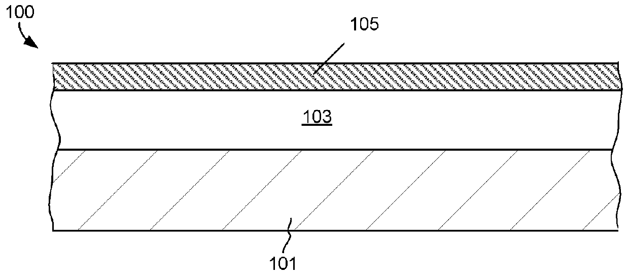
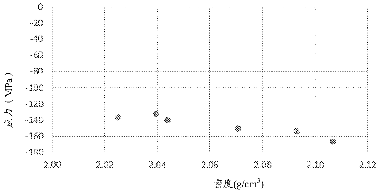

Image

  • Low temperature formation of high quality silicon oxide films in semiconductor device manufacturing
  • Low temperature formation of high quality silicon oxide films in semiconductor device manufacturing
  • Low temperature formation of high quality silicon oxide films in semiconductor device manufacturing

Examples


Embodiment 1

[0089] Example 1. Formation of a silicon oxide film with low stress and high density.

[0090] A number of silicon oxide films were deposited by PECVD on flat 300 mm wafers in a Vector PECVD reactor available from Lam Research Corporation, Fremont CA, at a temperature of 180° C. and a pressure of 2.5 Torr to 3.5 Torr. The process gas used during deposition consists of SiH 4 (provided at 30sccm), CO 2 (provided at 4200 sccm) and He composition. The plasma is generated in the process gas using 13.56MHz HF RF at a power level of 100-400W. Deposition proceeds for 5 seconds; then stops SiH 4 and CO 2 flow into the processing chamber while plasma and helium flows are maintained for 5 seconds to 4 and CO 2 Purge out of chamber. Next, the plasma power was increased to 500-1000 W and the helium flow rate was increased to 1000-4000 sccm, and the deposited silicon oxide film was subjected to plasma treatment for 6-20 seconds under these conditions. The temperature and pressure of...

Embodiment 2

[0091] Example 2. Structure of the formed low stress film.

[0092]Acquisition of FT IR spectra of low stress silicon oxide materials. Films were formed as described in Example 1 using the following process parameters: temperature 180 °C, pressure 3.5 Torr, plasma power 100 W (generated at 13.56 Mhz), SiH 4 Flow rate 30sccm, CO 2 Flow rate 4200 seem and He flow rate 1250 seem. The stress of the formed film is less than -40 MPa. It can be seen that the FT IR spectrum at about 2250cm -1 There is no Si-H peak at , which is usually present in silicon oxide films deposited by low-temperature PECVD without plasma post-treatment. This indicates that the plasma post-treatment reduces the hydrogen concentration in the formed film.

Embodiment 3

[0093] Example 3. Improvement of stress, density and RI by plasma post-treatment.

[0094] Silicon oxide films were deposited by low-temperature PECVD to a thickness of 411 angstroms, and their stress, density, and RI were measured. 30 sccm of SiH at a temperature of 180°C and a pressure of 3.5 Torr using a plasma power of 100W (13.56Mhz) 4 Flow Rate, 4200sccm CO 2 flow rate and a He flow rate of 1250 seem for deposition.

[0095] Another silicon oxide film was deposited by low-temperature PECVD using the same process conditions as those used in the deposition of the comparative film above, and then at a temperature of 180° C. using a plasma power of 500 W (13.56 Mhz) and a He flow rate of 1000 sccm, Plasma treatment was performed at a pressure of 3.5 Torr. The stress, density and RI of the treated films were measured.

[0096] Parameters for the comparative and treated membranes are provided in Table 4.

[0097] Table 4. Improvement in stress, density and RI upon plasma ...


PUM

PropertyMeasurementUnit
densityaaaaaaaaaa
compressive stressaaaaaaaaaa
densityaaaaaaaaaa

Abstract

Silicon oxide layer is deposited on a semiconductor substrate by PECVD at a temperature of less than about 200 DEG C and is treated with helium plasma to reduce stress of the deposited layer to an absolute value of less than about 80 MPa. Plasma treatment reduces hydrogen content in the silicon oxide layer, and leads to low stress films that can also have high density and low roughness. In some embodiments, the film is deposited on a semiconductor substrate that contains one or more temperature-sensitive layers, such as layers of organic material or spin-on dielectric that cannot withstand temperatures of greater than 250 DEG C. In some embodiments the silicon oxide film is deposited to a thickness of between about 100-200 angstroms, and is used as a hard mask layer during etching of otherlayers on a semiconductor substrate.

Description

[0001] Cross References to Related Applications [0002] This application claims the benefit of and priority to US Application Serial No. 15 / 280,049, filed September 29, 2016, designating McLaughlin et al. as inventor, the entire contents of which are incorporated herein by reference. technical field [0003] The present invention relates to methods of forming layers of material on semiconductor substrates. In particular, the present invention relates to methods of forming silicon oxide layers by plasma enhanced chemical vapor deposition (PECVD). Background technique [0004] The fabrication of semiconductor devices typically involves the deposition and patterning of several layers of different materials. When multiple layers are deposited in a stack, the stress characteristics of the deposited layers become particularly important, as highly stressed materials can cause disruption of layer alignment in the stack, bowing, delamination, and eventually patterning Inaccurate, ...

Claims


Application Information

Patent Timeline
Patent Type & Authority Applications(China)
IPC IPC(8): H01L21/02H01L21/324C23C16/455
CPCH01L21/31144C23C16/45523C23C16/505C23C16/402C23C16/56H01L21/02164H01L21/02211H01L21/02274H01L21/0234H01L21/02348H01L21/0274H01L21/3081H01L21/3086
Inventor 凯文·M·麦克劳克林阿米特·法尔克亚卡普·瑟里什·雷迪
Owner LAM RES CORP
Learn More