Thin film transistor and its manufacturing method, array substrate and display device

A technology of thin film transistors and substrates, applied in transistors, semiconductor/solid-state device manufacturing, semiconductor devices, etc., can solve problems such as poor performance of LTPSTFT, reduce large leakage current, high carrier mobility, and improve performance. Effect

Active Publication Date: 2021-01-26
BOE TECH GRP CO LTD +1
View PDF4 Cites 0 Cited by
  • Summary
  • Abstract
  • Description
  • Claims
  • Application Information

AI Technical Summary

Problems solved by technology

[0005] The embodiment of the present invention provides a thin film transistor and its manufacturing method, an array substrate and a display device, which can solve the problem of poor performance of LTPS TFT in the related art

Method used


Image

  • Thin film transistor and its manufacturing method, array substrate and display device
  • Thin film transistor and its manufacturing method, array substrate and display device
  • Thin film transistor and its manufacturing method, array substrate and display device

Examples


Embodiment Construction

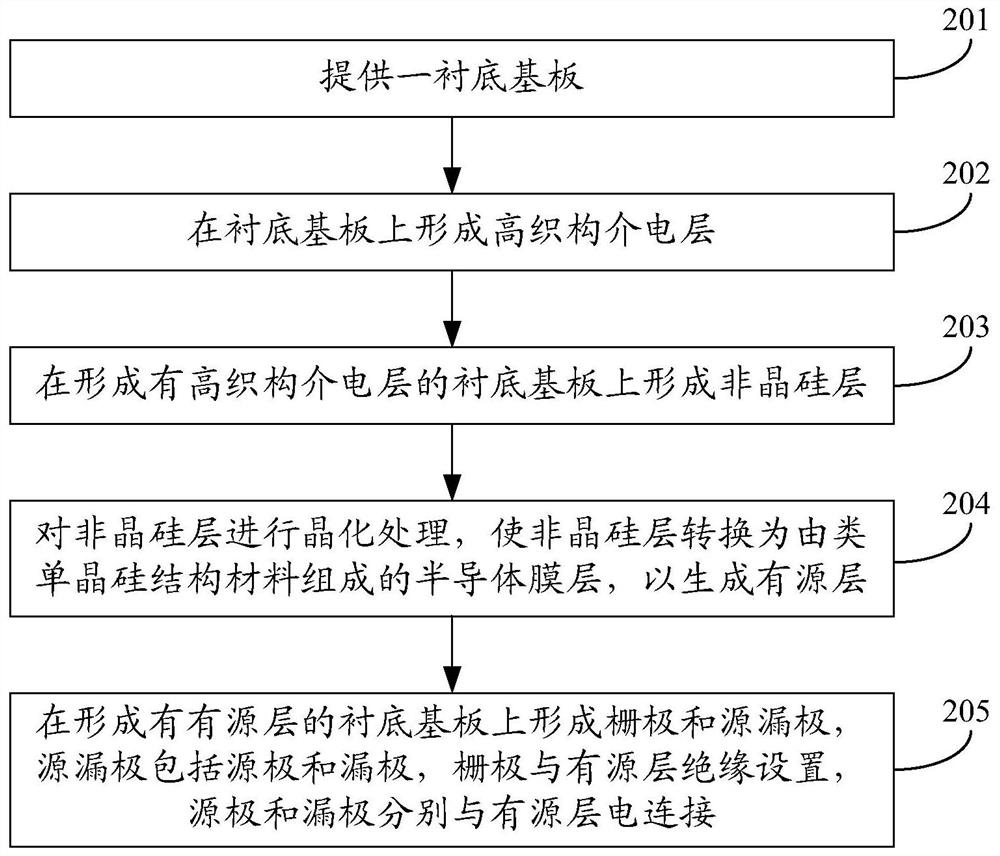
[0044] In order to make the object, technical solution and advantages of the present invention clearer, the implementation manner of the present invention will be further described in detail below in conjunction with the accompanying drawings.

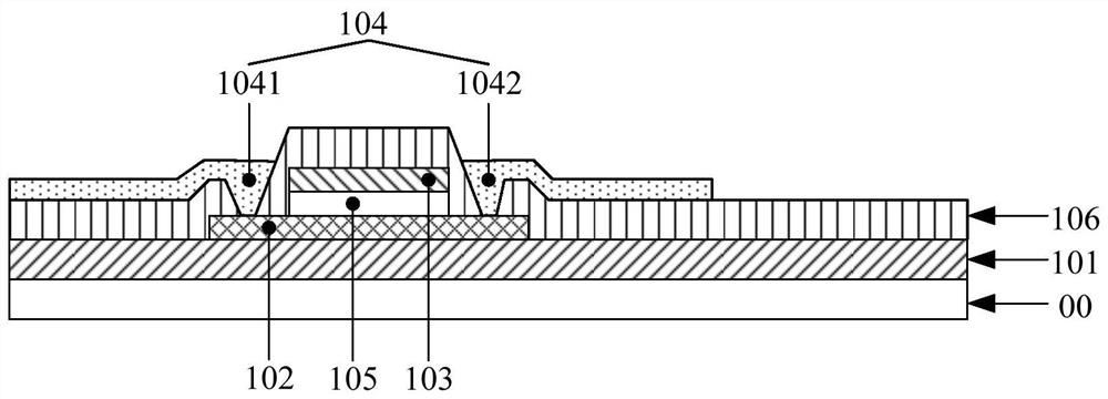
[0045] figure 1 It is a schematic structural diagram of a thin film transistor provided by an embodiment of the present invention. Such as figure 1 As shown, the thin film transistor 10 includes:

[0046] The highly textured dielectric layer 101, the active layer 102, the gate 103 and the source and drain 104 are stacked on the base substrate 00, the source and drain 104 includes the source 1041 and the drain 1042, the gate 103 and the active The layer 102 is insulated, and the source 1041 and the drain 1042 are electrically connected to the active layer 102 respectively.

[0047] Wherein, the active layer is a semiconductor film layer composed of a single-crystal silicon-like structure material. In the semiconductor film layer com...


PUM


Abstract

The invention discloses a thin film transistor, a manufacturing method thereof, an array substrate and a display device, and belongs to the field of display technology. It includes: a highly textured dielectric layer stacked on the base substrate, an active layer, a gate and a source and drain, the source and drain include a source and a drain, and the gate and the active layer Insulated, the source and the drain are electrically connected to the active layer respectively; wherein, the constituent particles of the active layer are single-crystal silicon-like structures. The invention replaces the original buffer layer with a highly textured dielectric layer to induce the active layer to grow into a single-crystal silicon-like structure, thereby improving the performance of the thin film transistor.

Description

technical field [0001] The invention relates to the field of display technology, in particular to a thin film transistor and a manufacturing method thereof, an array substrate and a display device. Background technique [0002] A display panel generally includes a plurality of pixel units, and each pixel unit is provided with a thin film transistor (ThinFilm Transistor, TFT). TFT is a basic circuit element that controls the display brightness of the corresponding pixel unit. The TFT may include: a buffer layer, an active layer, a gate insulating layer, a gate electrode, a source and a drain, and the like stacked on a substrate. The source and drain electrodes include a source electrode and a drain electrode, and the active layer provides a conductive channel for the source electrode and the drain electrode. Among them, the buffer layer is usually made of silicon nitride (SiN x ) or silicon oxide (SiO 2 ), the active layer is an amorphous silicon layer in a traditional am...

Claims


Application Information

Patent Timeline
Patent Type & Authority Patents(China)
IPC IPC(8): H01L29/786H01L21/336
CPCH01L21/02488H01L21/02494H01L21/02532H01L21/02592H01L21/02598H01L21/02491H01L21/02505H01L21/02516H01L21/02609H01L21/02686H01L29/78672H01L29/66757H01L29/66765H01L21/02175H01L21/02189H01L21/02266H01L27/1214H01L29/66772H01L29/78603H01L29/78654
Inventor 贵炳强曲连杰齐永莲赵合彬邱云
Owner BOE TECH GRP CO LTD
Why Eureka
Try Eureka