Microwave receiving and transmitting assembly
A technology for transmitting and receiving components and microwaves, which is applied in the direction of electrical components, printed circuit components, and electrical connection printed components, etc. It can solve problems such as failure of microwave and millimeter wave components, high transportation and use costs, and weak joint force capacity. Achieve miniaturized design, compact structure, and weight reduction
- Summary
- Abstract
- Description
- Claims
- Application Information
AI Technical Summary
Problems solved by technology
Method used
Image

Examples
Embodiment 1
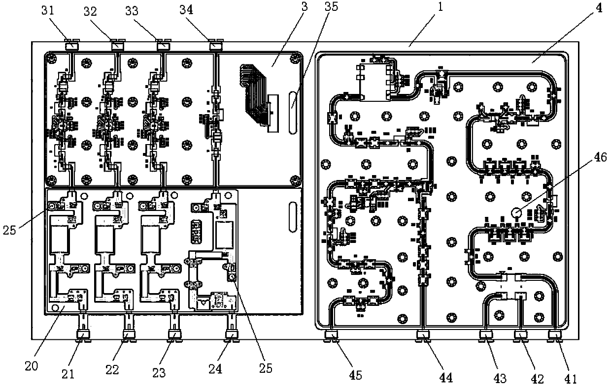
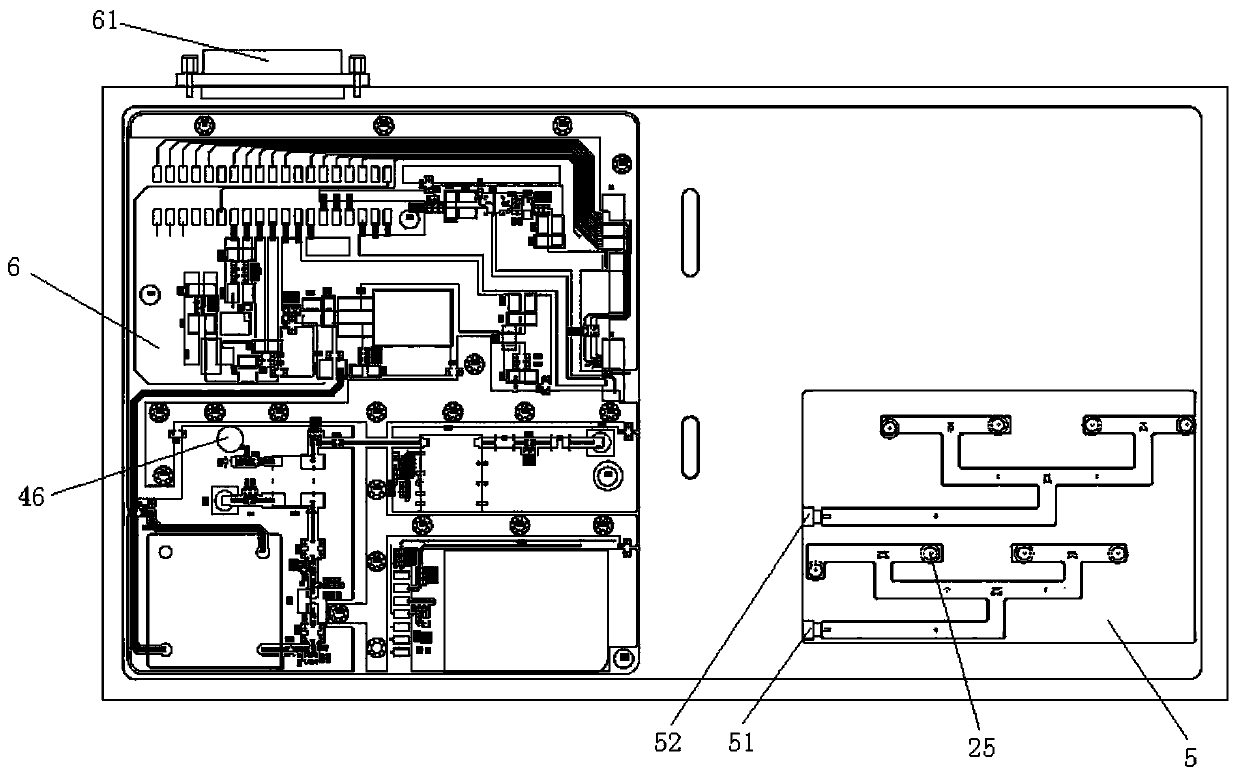
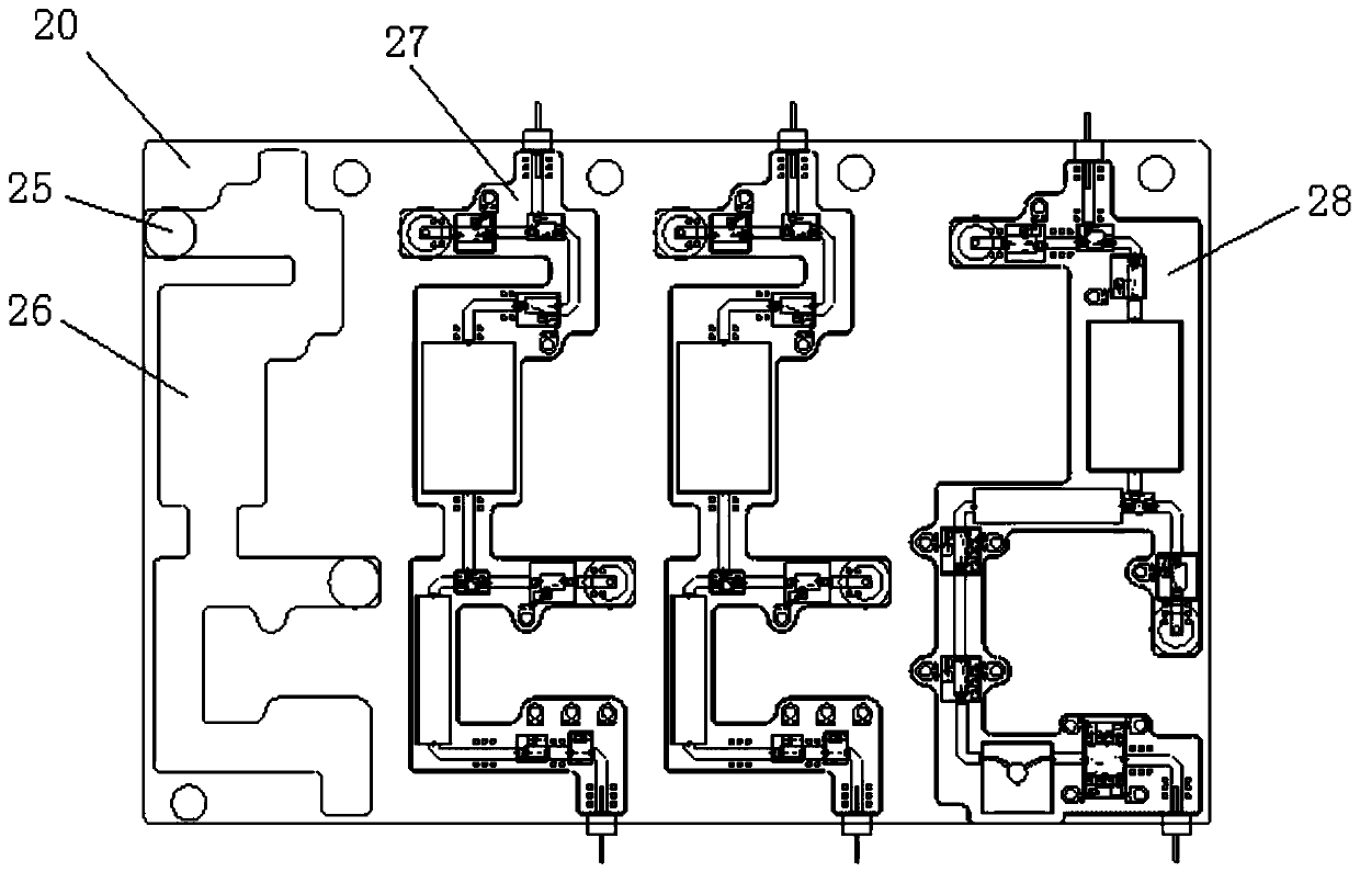
[0026] see Figure 1 to Figure 5 , in this embodiment, a microwave transceiver assembly includes a housing 1, a receiving input module, a receiving and output circuit board 3, a waveform output circuit board 4, a signal distribution circuit module, and a power supply and control circuit board 6, the housing 1 The top surface of the casing 1 is provided with a first groove and a second groove, the bottom surface of the housing 1 is provided with a third groove and a fourth groove, and the receiving input module and the receiving output circuit board 3 are arranged in the first concave Groove, the first groove is provided with a first receiving input interface 21, a second receiving input interface 22, a third receiving input interface 23 and a transmitting output interface 24 in order from left to right on the groove wall on one side of the receiving input module. A groove is provided with a first receiving output interface 31, a second receiving output interface 32, a third re...
Embodiment 2
[0033] On the basis of Embodiment 1, the receiving input circuit board 27 , the receiving output circuit board 3 , the waveform output circuit board 4 and the signal distribution circuit module of the receiving input module are all provided with bare chip hollowed out parts.
[0034] In this embodiment, the volume of the chip after packaging is relatively large, and the circuit board carrying the chip also needs to leave space for the chip, so that the volume and quality of the circuit board itself are relatively large, so the direct connection between the bare chip and the circuit board is adopted. The design method can greatly save the occupied area of the circuit board and realize the miniaturization design of the circuit board.
Embodiment 3
[0036]On the basis of Embodiment 2, the groove bottoms of the first groove, the second groove and the third groove correspond to the receiving input module, the receiving output circuit board 3, the waveform output circuit board 4 and the signal distribution circuit module The hollowed out parts of the heat sink are respectively provided with heat sink grooves, and each heat sink groove is provided with a heat sink 11, and each heat sink 11 is provided with a bare chip 12, and the projected area of the heat sink 11 is larger than the projected area of the bare chip 12 .
[0037] In this embodiment, in order to fix the bare chip conveniently, the bare chip is welded on the heat sink, which can effectively fix the bare chip, and can conduct the heat emitted by the chip to the shell in time, and the size of the heat sink is smaller than that of the bare chip. The size is about tens of microns larger, which greatly reduces the occupied area of the chip, and the heat sink is ...
PUM
 Abstract
Description
Claims
Application Information
 - R&D Engineer
- R&D Manager
- IP Professional
- Industry Leading Data Capabilities
- Powerful AI technology
- Patent DNA Extraction
Browse by: Latest US Patents, China's latest patents, Technical Efficacy Thesaurus, Application Domain, Technology Topic.
© 2024 PatSnap. All rights reserved.Legal|Privacy policy|Modern Slavery Act Transparency Statement|Sitemap