Array substrate and manufacturing method thereof

A technology for array substrates and manufacturing methods, applied in the direction of exposure devices, optics, instruments, etc. in photolithography, can solve the problems of increased process steps and lower yields, and achieve cost savings, large pixel aperture ratios, and reduced number of masks Effect

Inactive Publication Date: 2019-05-31
NANJING CEC PANDA FPD TECH CO LTD +2
View PDF6 Cites 3 Cited by
  • Summary
  • Abstract
  • Description
  • Claims
  • Application Information

AI Technical Summary

Problems solved by technology

In actual production, to realize the purpose of this patent, each layer of thin film transistors needs to go through a completely independent manufacturing process, which greatly increases the number of process steps and reduces the yield rate.

Method used


Image

  • Array substrate and manufacturing method thereof
  • Array substrate and manufacturing method thereof
  • Array substrate and manufacturing method thereof

Examples


Embodiment 1

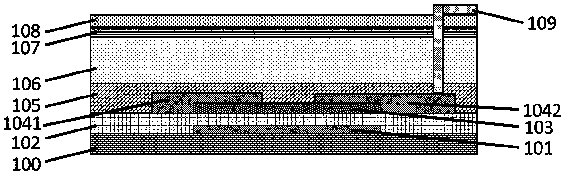
[0046]The array substrate of the present invention includes: criss-cross scan lines and data lines, a pixel area defined by intersections of the scan lines and data lines, a thin film transistor located in the pixel area, and a planarization layer 06 . The thin film transistor is a multi-layer thin film transistor, that is, in the same projected area (x / y plane), at least two thin film transistors arranged one above the other in the z space are provided.

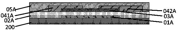
[0047] Such as figure 2 As shown, the multilayer thin film transistor in this embodiment includes a first thin film transistor located on the base substrate 200, and a second thin film transistor located above the first thin film transistor, and the planarization layer 06 is located between the first thin film transistor and the second thin film transistor. between thin film transistors. The first thin film transistor includes, from bottom to top: a first gate 01A located on the substrate 200, a first gate insulating layer...

Embodiment 2

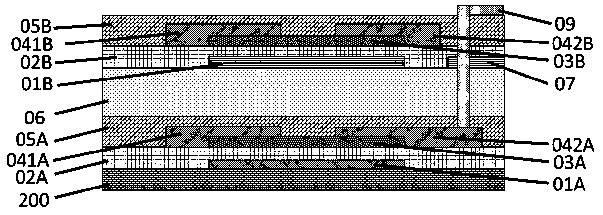
[0077] Figure 7 Shown is a schematic structural diagram of an array substrate according to Embodiment 2 of the present invention. The difference from Embodiment 1 is that both the first thin film transistor and the second thin film transistor in the multilayer thin film transistor of Embodiment 1 adopt a bottom gate structure. Both the first thin film transistor and the second thin film transistor in the multilayer thin film transistor of the embodiment adopt a top-gate structure.

[0078] It should be noted that the multi-layer thin film transistor of the array substrate of the present invention includes a plurality of thin film transistors arranged in layers above and below in the z space, and the plurality of thin film transistors can be independently set as top gates, bottom gates, BCE (back channel channel etching type), ESL (channel protection type) and other transistor types.

[0079] Such as Figure 7 As shown, the multilayer thin film transistor in this embodiment ...


PUM

PropertyMeasurementUnit
thicknessaaaaaaaaaa
thicknessaaaaaaaaaa
thicknessaaaaaaaaaa

Abstract

The invention provides an array substrate and a manufacturing method thereof, and belongs to the technical field of display. The array substrate comprises a multilayer thin film transistor and a planarization layer, wherein the multilayer thin film transistor comprises a first thin film transistor and a second thin film transistor; the planarization layer is positioned between the first thin filmtransistor and the second thin film transistor; and a common electrode of the first thin film transistor and a grid electrode of the second thin film transistor are formed by adopting the same layer of a transparent conductive material. According to the array substrate, at least two laminated thin film transistors are arranged in a same projection area, so that the display can realize the functions of pixel self-driving, ultra-narrow frame and the like while maintaining a larger pixel aperture ratio; and the common electrode of the first thin film transistor and the grid electrode of the second thin film transistor are formed by the same layer of the transparent conductive material, so that the number of masks and the cost are saved.

Description

technical field [0001] The invention belongs to the field of display technology, and in particular relates to an array substrate and a manufacturing method thereof. technical background [0002] The multi-functionalization of consumer electronics requires that the number of individual electronic devices gradually increase, while the size gradually decreases. However, the design of high-density thin film transistors in a planar space poses challenges to the process and stability. [0003] The existing array substrate structures using single-layer thin film transistors are as follows: figure 1 As shown, there is only one thin film transistor in a projected area. The array substrate includes from bottom to top: a gate 101 located on the base substrate 100, a gate insulating layer 102, an active layer 103, a source 1041 and a drain 1042 in contact with the active layer 103, a first insulating layer 105 , planarization layer 106 , common electrode 107 , second insulating layer...

Claims


Application Information

Patent Timeline
Patent Type & Authority Applications(China)
IPC IPC(8): G02F1/13G02F1/1362G03F7/20H01L27/12
Inventor 徐尚君王鸣昕王利忠王怀佩舒扬周刘飞王志军
Owner NANJING CEC PANDA FPD TECH CO LTD
Why Eureka
Try Eureka